Method for forming a semiconductor device

a technology of memory devices and semiconductors, applied in the direction of semiconductor devices, basic electric elements, electrical equipment, etc., can solve the problems of increasing the breakdown rate, increasing the difficulty of process control, and increasing the parameters of etching processes for various materials

Active Publication Date: 2010-12-21
NAN YA TECH
View PDF6 Cites 0 Cited by
  • Summary
  • Abstract
  • Description
  • Claims
  • Application Information

AI Technical Summary

Benefits of technology

[0006]One aspect of the present invention is to provide a method for forming a semiconductor device, which includes forming a spacer with a well-controlled pattern profile to avoid the edge damage of the gate conductor, where the edge damage inevitably occurs in the conventional processes.
[0007]Another aspect of the present invention is to provide a method for forming a semiconductor device, which has floating gates with a good profile control on two sides of the control gate, so that the coupling ratio is effectively increased and the performance of the semiconductor device is improved.
[0008]A further aspect of the present invention is to provide a method for forming a semiconductor device, which reduces the width of the mask layer to a desired level to self-alignedly define the floating gate of the memory device.

Problems solved by technology

However, as the feature size of the semiconductor device reduces, the complexity of conventional methods, and the parameters of etching processes for various materials become more and more difficult to control, such that the breakdown rate increases due to inappropriate control of etching rate or voltage.
However, because the spacer having a curved shape causes the etching process more difficult to control, the edge of the gate conductor may be damaged during the process of removing the spacer.

Method used


Image

  • Method for forming a semiconductor device
  • Method for forming a semiconductor device
  • Method for forming a semiconductor device

Examples


Embodiment Construction

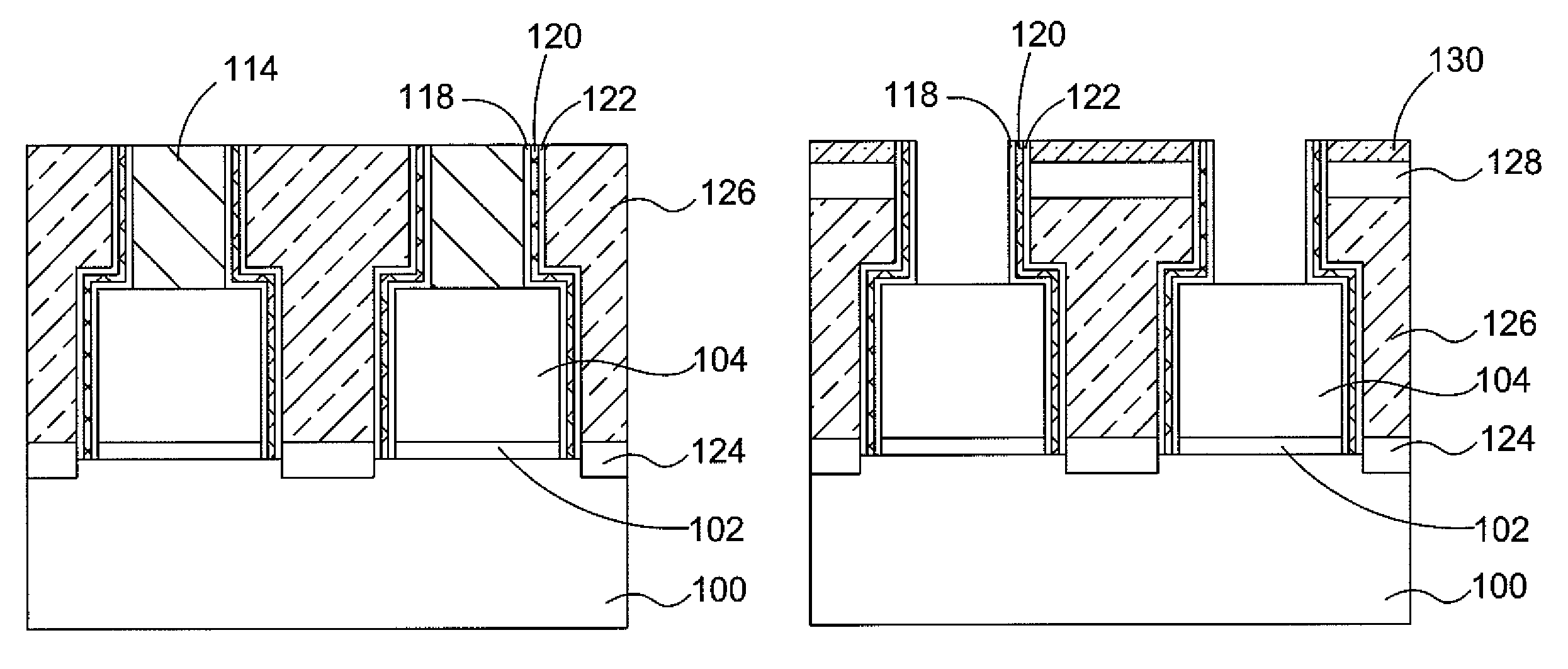
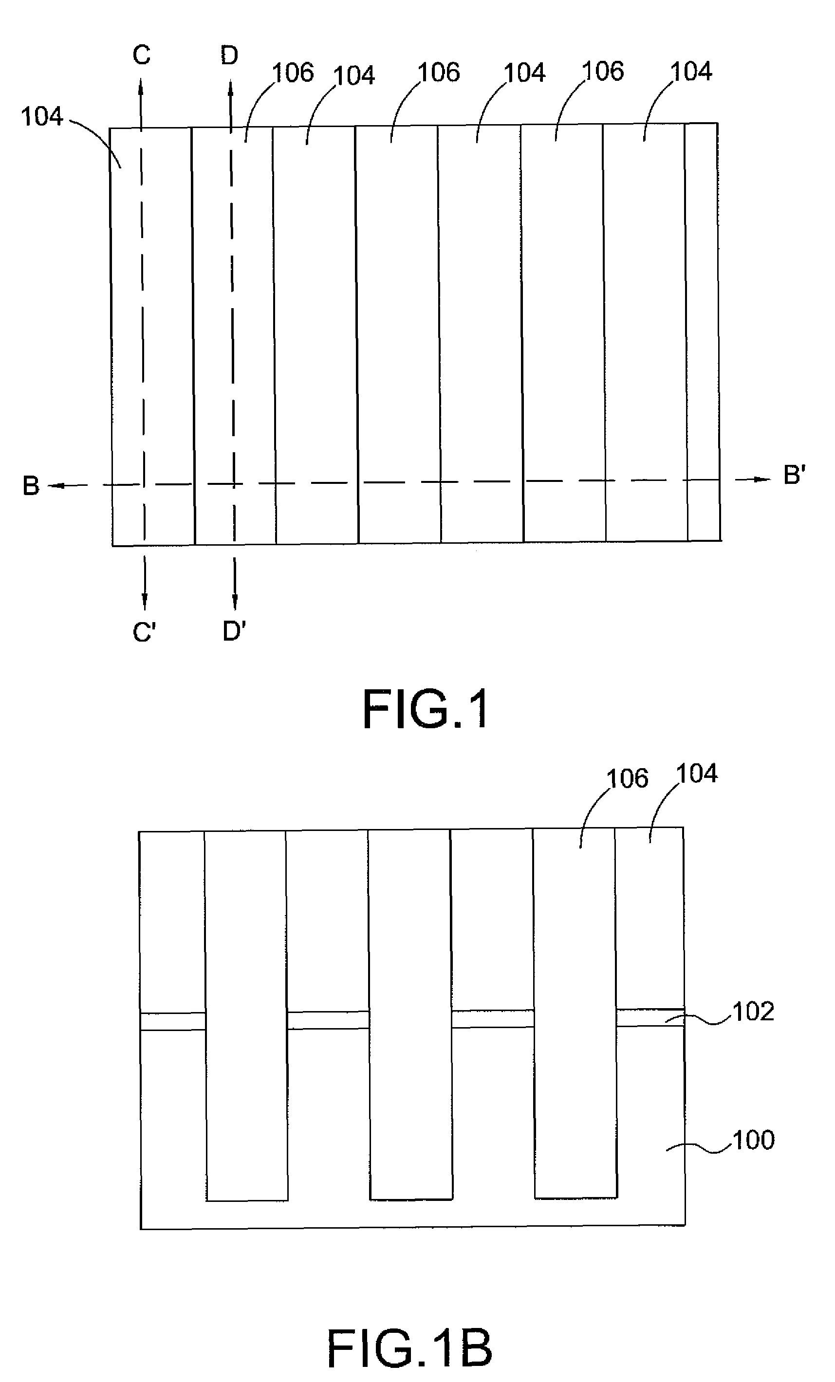
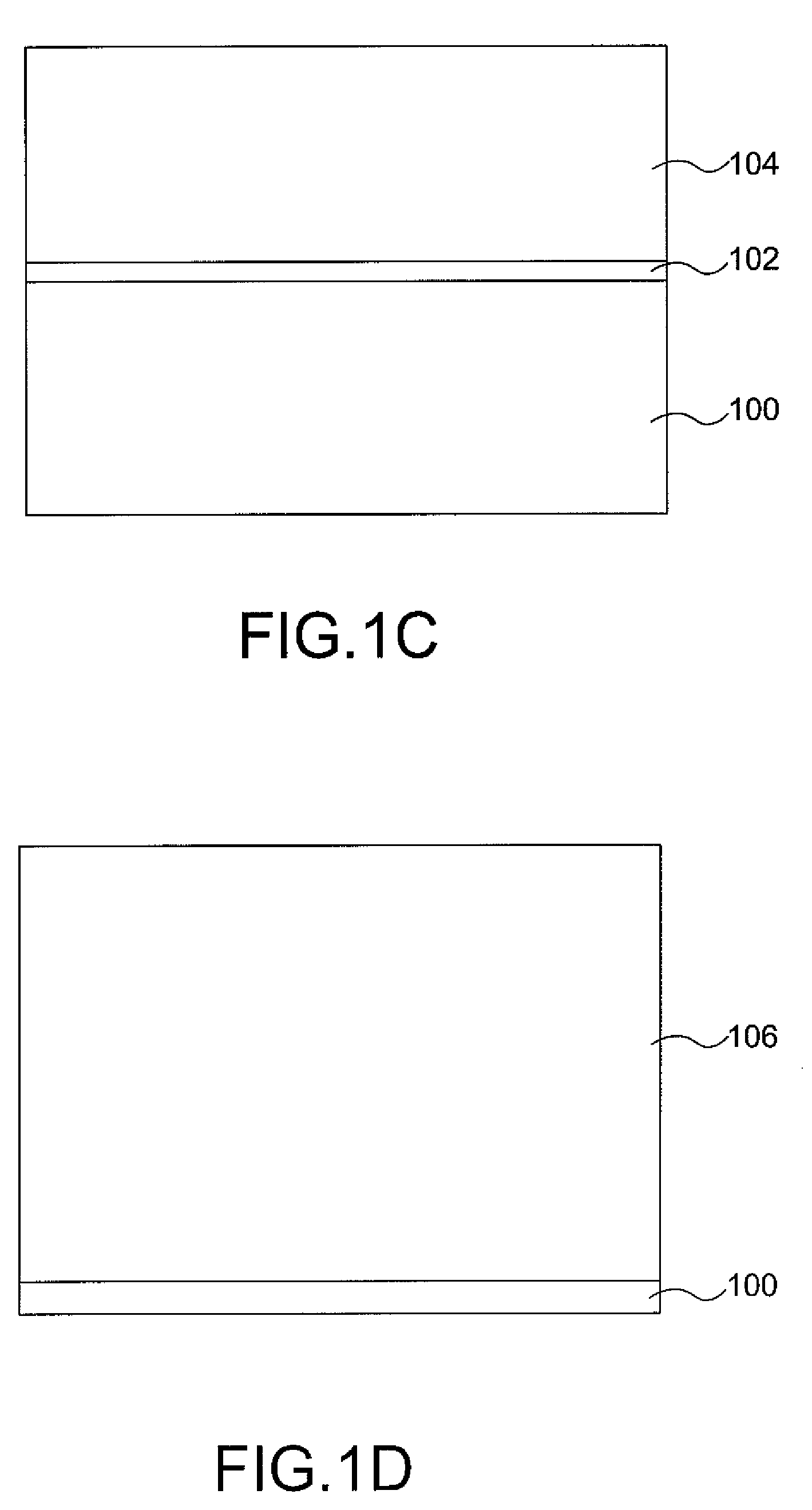
[0024]The present invention provides a method for forming a semiconductor device, which can avoid the edge damage of the gate conductor. The present invention will now be described in detail with reference to the attached drawings of FIG. 1 to FIG. 11. The description sets forth various preferred embodiments of the present invention only, and is not intended to limit the scope, applicability, or configuration of the invention in any way. The layers described below can be formed by conventional techniques including lithography (such as coating, exposing, developing, etc.), etching (such as dry etching, wet etching, reactive ion etching, etc.), deposition (such as chemical vapor deposition, physical vapor deposition, plasma enhanced deposition, etc.), thermal process (such as thermal oxidation, annealing, thermal diffusion, etc.), polishing (such as chemical mechanical polishing, etc.), and implant (such as ion implantation, etc.) and the likes, which are well known in the art and not...


PUM


Abstract

A method for forming a semiconductor device, includes the steps of providing a substrate; forming a patterned stack on the substrate including a first dielectric layer on the substrate, a first conductive layer on the first dielectric layer and a mask layer on the first conductive layer, wherein a width of the mask layer is smaller than a width of the first conductive layer; forming a second dielectric layer on the sidewall of the patterned stack; forming a third dielectric layer on the substrate; forming a second conductive layer over the substrate; and removing the mask layer and a portion of the first conductive layer covered by the mask layer to form an opening so as to partially expose the first conductive layer.

Description

CROSS REFERENCE TO RELATED APPLICATIONS[0001]This application claims the right of priority based on Taiwan Patent Application No. 96142983 entitled “Method for Forming Semiconductor Device,” filed on Nov. 14, 2007, which is incorporated herein by reference and assigned to the assignee herein.FIELD OF THE INVENTION[0002]The present invention relates to a method for forming a semiconductor device, and more particularly, relates to a method for forming a memory device.BACKGROUND OF THE INVENTION[0003]The fabrication of semiconductor circuits generally repeatedly performs a series of processes including lithography, deposition, etching, and the like to form layer-stacked integrated circuits. However, as the feature size of the semiconductor device reduces, the complexity of conventional methods, and the parameters of etching processes for various materials become more and more difficult to control, such that the breakdown rate increases due to inappropriate control of etching rate or vo...

Claims


Application Information

Patent Timeline
Patent Type & Authority Patents(United States)
IPC IPC(8): H01L21/76
CPCH01L21/823437H01L21/823468H01L21/823481H01L27/11521H01L21/28273H01L29/40114H10B41/30
Inventor TSAI, HUNG-MINGHSIAO, CHING-NANHUANG, CHUNG-LIN
Owner NAN YA TECH
Why Eureka
Try Eureka