Display device including data conversion circuit

a data conversion circuit and display device technology, applied in semiconductor devices, electrical devices, instruments, etc., can solve the problems of increasing power consumption and difficulty in high-speed processing, and achieve the effect of high-speed image processing and low power consumption

Active Publication Date: 2020-12-15
SEMICON ENERGY LAB CO LTD
View PDF47 Cites 0 Cited by
  • Summary
  • Abstract
  • Description
  • Claims
  • Application Information

AI Technical Summary

Benefits of technology

[0008]An object of one embodiment of the present invention is to provide a data conversion circuit and a display device that are capable of high-speed image processing. Another object of one embodiment of the present invention is to provide a data conversion circuit and a display device that have low power consumption. Another object of one embodiment of the present invention is to provide a novel data conversion circuit and a novel display device.
[0016]According to one embodiment of the present invention, a data conversion circuit and a display device that are capable of high-speed image processing can be provided. According to one embodiment of the present invention, a data conversion circuit and a display device that have low power consumption can be provided. According to one embodiment of the present invention, a novel data conversion circuit and a novel display device can be provided.

Problems solved by technology

Image processing by software requires processing of the entire frame, and thus has difficulty in high-speed processing.
The use of a large frame memory and high-throughput graphics processing unit (GPU) enables high-speed image processing; however, this increases power consumption.

Method used


Image

  • Display device including data conversion circuit
  • Display device including data conversion circuit
  • Display device including data conversion circuit

Examples


embodiment 1

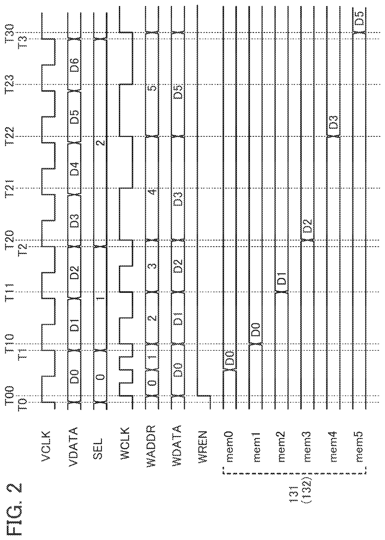
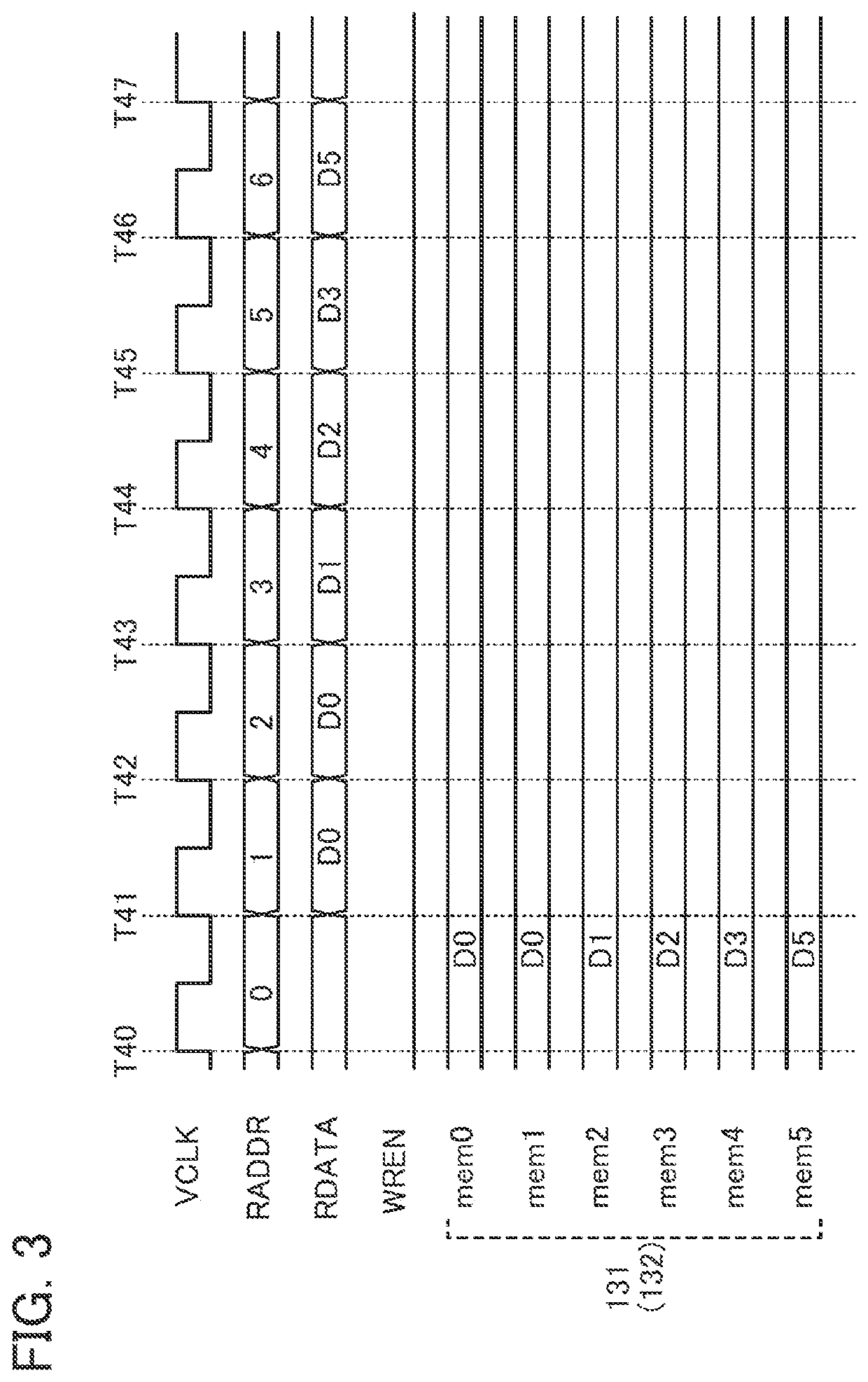
[0045]This embodiment will describe structure examples of a data conversion circuit of one embodiment of the present invention and a display device including the data conversion circuit with reference to FIG. 1 to FIG. 5.

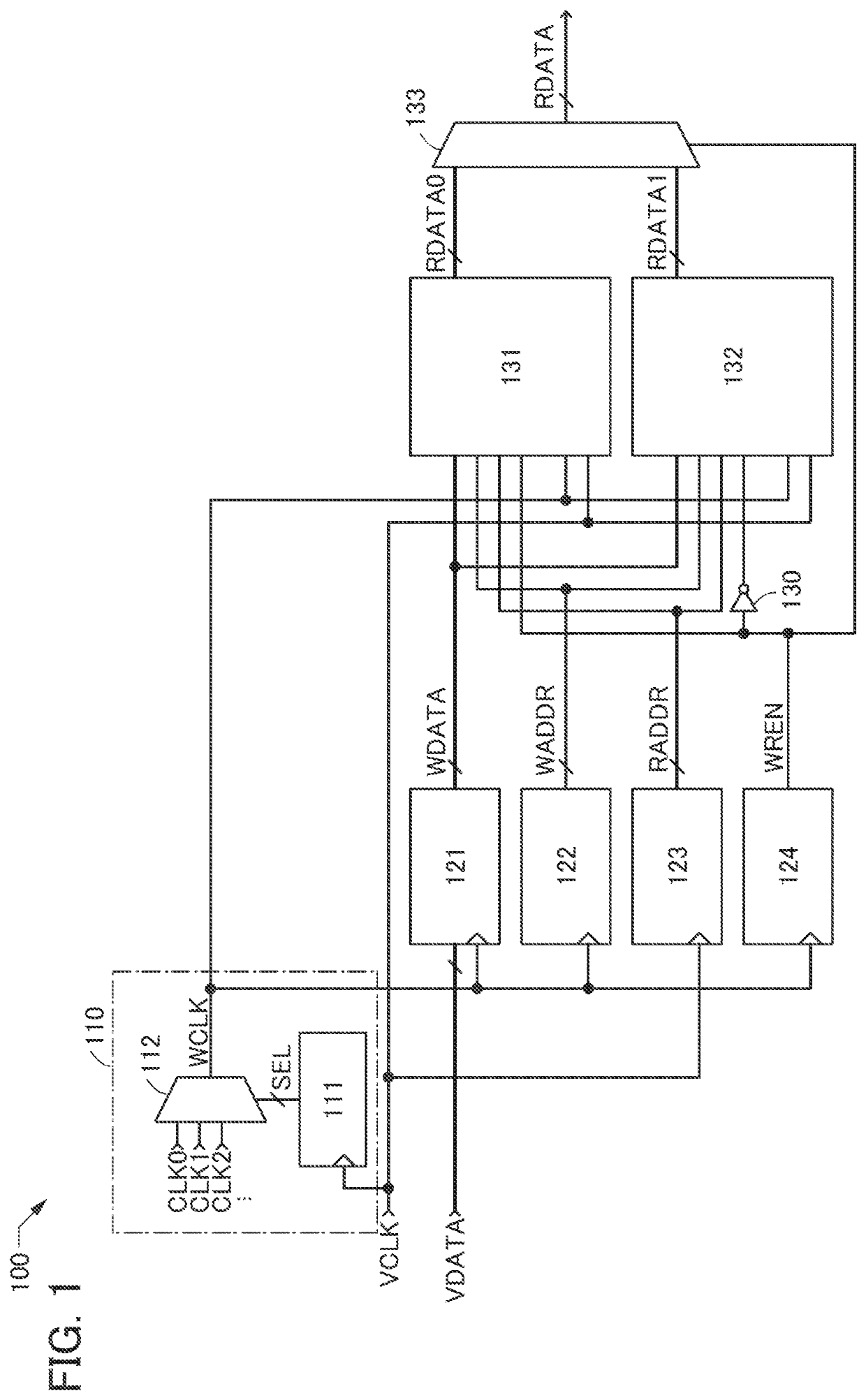
[0046]FIG. 1 is a block diagram of a data conversion circuit 100 of one embodiment of the present invention. The data conversion circuit 100 generates converted data for correcting image distortion due to a shape folded in the long axis direction of a source driver of a display device.

[0047]The data conversion circuit 100 includes a clock generation circuit 110, a data latch circuit 121, a writing address generation circuit 122, a readout address generation circuit 123, an enable generation circuit 124, a memory circuit 131, a memory circuit 132, and a data selection circuit 133.

[0048]The clock generation circuit 110 includes a clock selection control circuit 111 and a switching circuit 112. The clock selection control circuit 111 outputs a selection signal SEL with...

embodiment 2

[0090]The combination use of the data conversion circuit 100 of FIG. 1 and the data conversion circuit 140 of FIG. 4 that are described in the above embodiment enables correction of image distortion in both the long axis direction of the source driver and the long axis direction of the gate driver. Such combination allows image correction due to any shape distortion in the display device.

[0091]For example, such correction can be performed by supplying the data RDATA to the source driver 170 through the data conversion circuit 100 of FIG. 1, as shown in a display device 195 of FIG. 7. In addition, such correction can be performed by supplying the signals GPWC, GSP, and GCLK to the gate driver 180 through the data conversion circuit 140 of FIG. 4.

[0092]The above structure enables correction corresponding to a folded shape of the display device. This correction may be set by a user in advance. This correction may be performed on a real-time basis with real-time data of a folded shape o...

embodiment 3

[0106]In this embodiment, cross-sectional structure examples of a display device of one embodiment of the present invention will be described with reference to drawings.

Structure Example of Display Device

[0107]FIG. 11 is a schematic top view of a display device 10 described below. The display device 10 includes a pixel portion 11, a scan line driver circuit 12, a signal line driver circuit 13, a terminal portion 15, a plurality of wirings 16a, a plurality of wirings 16b, and the like.


PUM


Abstract

Image processing in accordance with the shape of a display device is performed at high speed with low power consumption, without the use of a large frame memory or a high-throughput GPU. Used is a data conversion circuit including: a latch circuit that takes in data from input data in synchronization with a writing clock signal and stores the data as writing data; a memory circuit that stores the writing data and outputs the writing data to an external circuit as readout data in synchronization with a readout clock signal; and a clock selection control circuit. The writing clock signal is one of a plurality of clock signals with different frequencies and is output in accordance with control by the clock selection control circuit.

Description

TECHNICAL FIELD[0001]One embodiment of the present invention relates to a data conversion circuit and a display device.BACKGROUND ART[0002]A curved display including an organic electroluminescent (EL) element has been proposed (see Patent Document 1, for example). Note that the curved display means a display including a curved display surface.[0003]It is expected that the use of the curved display for an instrument panel of a vehicle such as a car will lead to the design improvement (see Patent Document 2, for example).REFERENCEPatent Reference[0004][Patent Document 1] Japanese Published Patent Application No. 2013-134295[0005][Patent Document 2] Japanese Published Patent Application No. 2005-112251DISCLOSURE OF INVENTION[0006]An instrument panel of a car or the like has a complex (e.g., curved) shape in view of design. When a user sees information on the display device with such a shape, sight lines of the user and the display surface make inconstant angles. That is, the position o...

Claims


Application Information

Patent Timeline
Patent Type & Authority Patents(United States)
IPC IPC(8): G09G5/00G09G3/32G09G3/3275G09G3/3266
CPCG09G3/3275G09G5/005G09G3/3266G09G2380/10G09G2310/08G09G2320/0252G09G2380/02G09G2340/14G09G3/32G09G3/20G09G3/3225G09G3/2096G09G2310/0286G09G2320/0233G09G2340/0421G09G2310/0205G09G2340/0414H01L27/1225H01L27/1266G09G3/035
Inventor OKAMOTO, YUKIYONEDA, SEIICHI
Owner SEMICON ENERGY LAB CO LTD
Why Eureka
Try Eureka