Data conversion circuit and display device
a data conversion circuit and display device technology, applied in the direction of electrical equipment, semiconductor devices, instruments, etc., can solve the problems of increasing power consumption and difficulty in high-speed processing, and achieve the effect of high-speed image processing and low power consumption
- Summary
- Abstract
- Description
- Claims
- Application Information
AI Technical Summary
Benefits of technology
Problems solved by technology
Method used
Image
Examples
embodiment 1
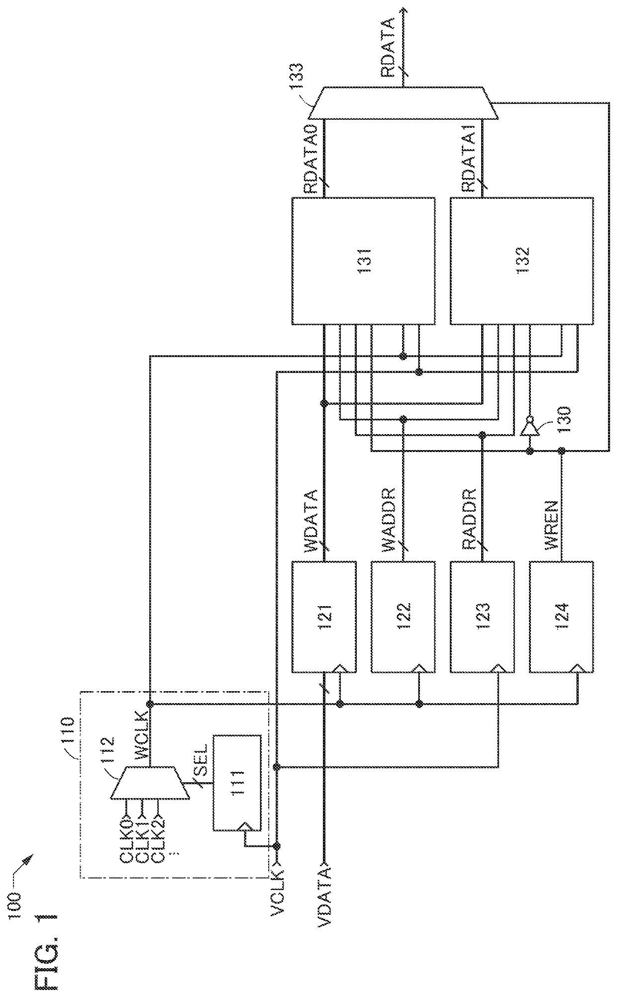
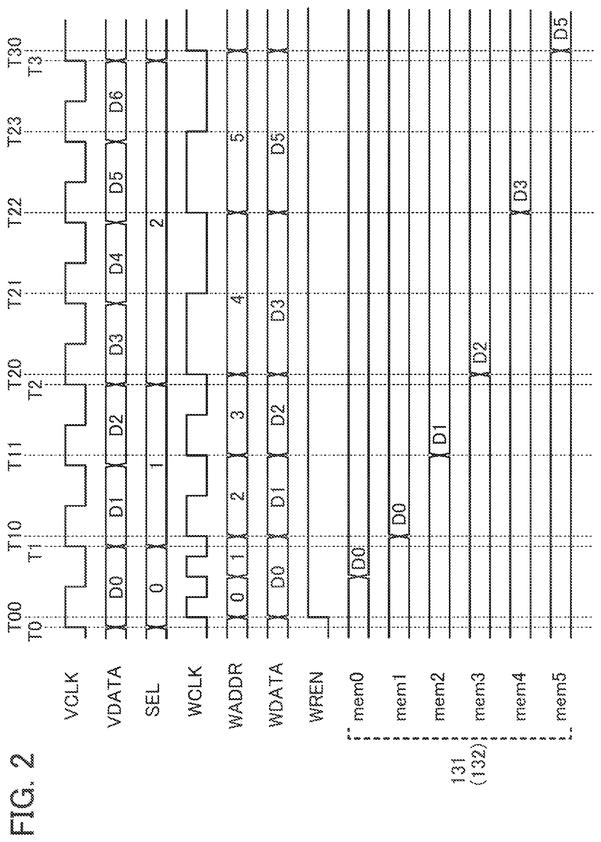
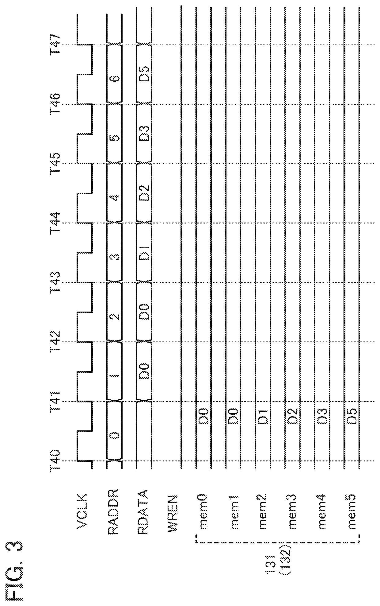
[0045]This embodiment will describe structure examples of a data conversion circuit of one embodiment of the present invention and a display device including the data conversion circuit with reference to FIG. 1 to FIG. 5.
[0046]FIG. 1 is a block diagram of a data conversion circuit 100 of one embodiment of the present invention. The data conversion circuit 100 generates converted data for correcting image distortion due to a shape folded in the long axis direction of a source driver of a display device.
[0047]The data conversion circuit 100 includes a clock generation circuit 110, a data latch circuit 121, a writing address generation circuit 122, a readout address generation circuit 123, an enable generation circuit 124, a memory circuit 131, a memory circuit 132, and a data selection circuit 133.
[0048]The clock generation circuit 110 includes a clock selection control circuit 111 and a switching circuit 112. The clock selection control circuit 111 outputs a selection signal SEL with...
embodiment 2
[0090]The combination use of the data conversion circuit 100 of FIG. 1 and the data conversion circuit 140 of FIG. 4 that are described in the above embodiment enables correction of image distortion in both the long axis direction of the source driver and the long axis direction of the gate driver. Such combination allows image correction due to any shape distortion in the display device.
[0091]For example, such correction can be performed by supplying the data RDATA to the source driver 170 through the data conversion circuit 100 of FIG. 1, as shown in a display device 195 of FIG. 7. In addition, such correction can be performed by supplying the signals GPWC, GSP, and GCLK to the gate driver 180 through the data conversion circuit 140 of FIG. 4.
[0092]The above structure enables correction corresponding to a folded shape of the display device. This correction may be set by a user in advance. This correction may be performed on a real-time basis with real-time data of a folded shape o...
embodiment 3
[0106]In this embodiment, cross-sectional structure examples of a display device of one embodiment of the present invention will be described with reference to drawings.
Structure Example of Display Device
[0107]FIG. 11 is a schematic top view of a display device 10 described below. The display device 10 includes a pixel portion 11, a scan line driver circuit 12, a signal line driver circuit 13, a terminal portion 15, a plurality of wirings 16a, a plurality of wirings 16b, and the like.
PUM
 Abstract
Description
Claims
Application Information


