Organic electroluminescent device and illumination device

an electroluminescent device and organic technology, applied in the direction of electric lighting sources, solid-state devices, light sources of electric light sources, etc., can solve the problems of inability to achieve difficult to individually control the optical characteristics of the respective layers, and difficulty in achieving suitable optical design for optimizing the distribution characteristics of light emitted from the element into the substrate. achieve the effect of high luminous efficiency

Active Publication Date: 2020-12-29
XIANYANG CHVT NEW DISPLAY TECH CO LTD
View PDF30 Cites 0 Cited by
  • Summary
  • Abstract
  • Description
  • Claims
  • Application Information

AI Technical Summary

Benefits of technology

[0042]According to the one aspect described above, it is possible to provide an organic electroluminescent device which can provide white light with a high luminous efficiency by being optimized in total luminous flux and is thus suitable for a lighting device and also provide a lighting device including this organic electroluminescent device.

Problems solved by technology

However, when light is to be extracted to the outside through a substrate in the MPE element, it is difficult to appropriately control the distribution characteristics of light emitted from the element into the substrate and the technology has not yet reached the level where the light can be sufficiently extracted to the outside.
Accordingly, the MPE element has a problem that it is difficult to individually control the optical characteristics of the respective layers and a suitable optical design for optimizing the distribution characteristics of light emitted from the element into the substrate is not achieved.

Method used


Image

  • Organic electroluminescent device and illumination device
  • Organic electroluminescent device and illumination device
  • Organic electroluminescent device and illumination device

Examples


first embodiment

“Organic Electroluminescent Device (Organic EL Device)”

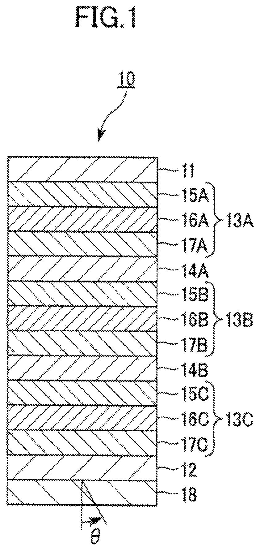
[0056]FIG. 1 is a cross-sectional view illustrating a schematic configuration of an organic EL device according to a first embodiment of the present invention.

[0057]As illustrated in FIG. 1, the organic EL device 10 of the embodiment has a structure in which multiple light emitting units 13A, 13B, 13C each including a light emitting layer made of at least an organic compound are stacked one on top of another between a first electrode 11 and a second electrode 12 with each of charge generating layers (CGL) 14A, 14B sandwiched between the corresponding pair of the adjacent light emitting units 13A, 13B, 13C. The organic EL device 10 is an organic EL device capable of providing white light through a substrate 18 adjacent to the second electrode 12 by causing the multiple light emitting units 13A, 13B, 13C to emit light.

[0058]Note that the organic EL device 10 of the embodiment may be an organic EL device capable of providing white ...

second embodiment

“Lighting Device”

[0118]An embodiment of the lighting device in the present invention is described.

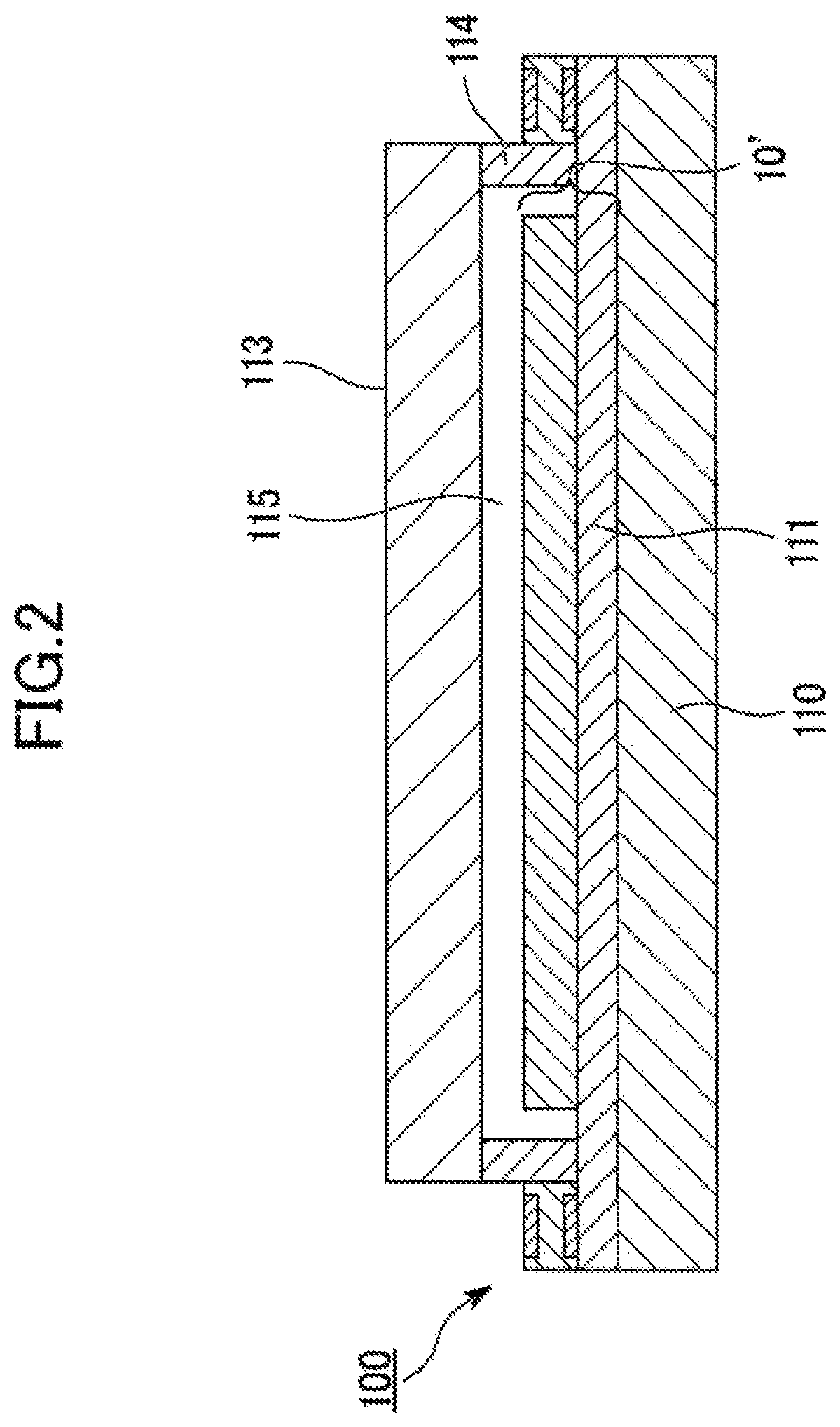
[0119]FIG. 2 is a cross-sectional view illustrating a configuration of one embodiment of the lighting device in the present invention. Although an example of the lighting device to which the present invention is applied is described herein, the lighting device of the present invention is not necessarily limited to such a configuration and various changes can be made as appropriate.

[0120]The lighting device 100 of the embodiment includes, for example, the organic EL device 10 in the aforementioned first embodiment as a light source. A base substrate 110 in the lighting device 100 of the embodiment corresponds to the substrate 18 in the organic EL element 10′ and anode terminal electrodes 111 in the lighting device 100 corresponds to the second electrode 12 in the organic EL device 10. The organic EL device 10 includes the organic EL element 10′ and the organic EL element 10′ is formed of...

example 1

“Manufacturing of Organic EL Device”

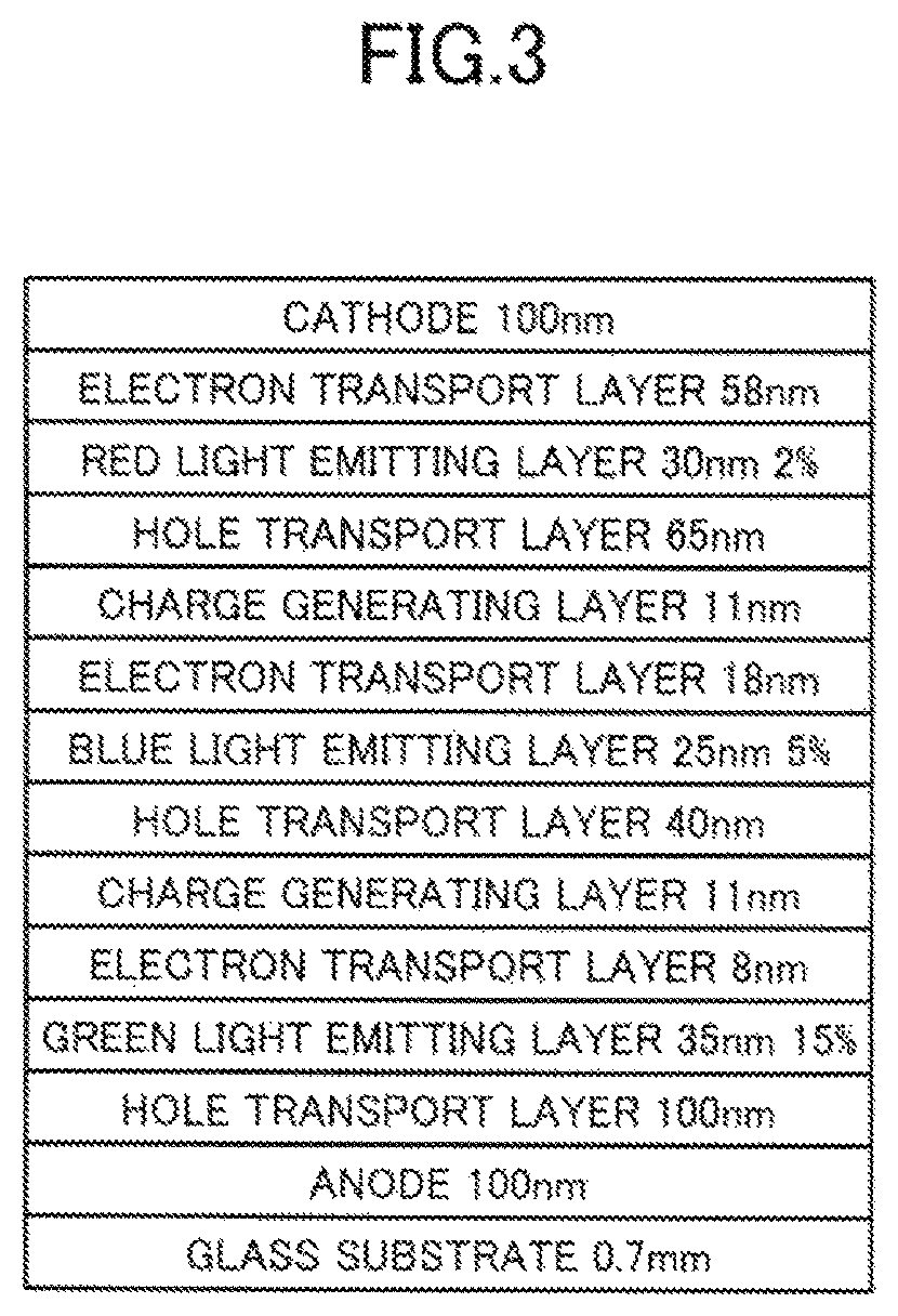
[0133]In Example 1, an organic EL device having a schematic structure illustrated in FIG. 3 was manufactured.

[0134]Specifically, first, there was prepared a soda-lime glass substrate with a thickness of 0.7 mm on which an ITO film with a thickness of 100 nm, a width of 2 mm, and a sheet resistance of about 20 Ω / □ was formed.

[0135]Then, the substrate was subjected to ultrasonic cleaning by using neutral detergent, ion-exchanged water, acetone, and isopropyl alcohol for 5 minutes for each cleaner and then subjected to spin drying and UV / O3 treatment.

[0136]Next, vapor deposition crucibles (made of tantalum or alumina) in a vacuum deposition apparatus were filled respectively with materials used to form layers illustrated in FIG. 3. Then, the substrate was set in the vacuum deposition apparatus, electric power was supplied to the vapor deposition crucibles to heat them in a reduced pressure atmosphere with a degree of vacuum of 1×10⁻⁴ Pa or less, and ...


PUM

PropertyMeasurementUnit
color rendering indexaaaaaaaaaa
wavelength bandaaaaaaaaaa

Abstract

An organic electroluminescent device wherein, among the distribution characteristics of light emitted inside a substrate: the brightness of white light has a maximum value within an angle range of 20-60° from an axis perpendicular to the planar direction of the substrate; the spectral radiance of red light at the maximum emission wavelength and the spectral radiance of green light at the maximum emission wavelength have maximum values within the angle range of 30-70° from the axis perpendicular to the planar direction of the substrate; and the maximum values are greater than the value for spectral radiance of red light at the maximum emission wavelength and the value for the spectral radiance of green light at the maximum emission wavelength, in the axial direction perpendicular to the planar direction of the substrate.

Description

TECHNICAL FIELD[0001]The present invention relates to an organic electroluminescent device and to a illumination device including the same.[0002]The present application claims the benefit of priority of Japanese Patent Application No. 2017-23309 filed on Feb. 10, 2017, the contents of which are incorporated herein by reference.BACKGROUND ART[0003]An organic electroluminescent element (hereafter, also referred to as “organic EL element” for short) is a self-luminescent element including a light emitting layer, made of an organic compound, between a cathode and an anode facing each other. When voltage is applied between the cathode and the anode, electrons injected into the light emitting layer from the cathode side and holes injected into the light emitting layer from the anode side recombine in the light emitting layer to form excitons and the excitons causes the organic EL element to emit light.[0004]As an organic EL element capable of achieving high luminance and longlife, there i...

Claims


Application Information

Patent Timeline
Patent Type & Authority Patents(United States)
IPC IPC(8): H01L51/50H01L51/52
CPCH01L51/5056H01L51/5072H01L51/504H05B33/02H05B33/12H05B33/26H10K59/32H10K50/131H10K50/19H10K50/13H10K50/15H10K50/16
Inventor TANAKA, JUNICHI
Owner XIANYANG CHVT NEW DISPLAY TECH CO LTD
Why Eureka
Try Eureka