Organic electroluminescent device and fabrication method thereof

a technology of organic electroluminescent devices and fabrication methods, which is applied in the field of display, can solve the problems of increasing the complexity of technology, requiring a lot of equipment expenditure for the fabrication of emission layers, etc., and achieve the effect of reducing equipment expenditur

Active Publication Date: 2020-12-29
WUHAN CHINA STAR OPTOELECTRONICS SEMICON DISPLAY TECH CO LTD +1
View PDF10 Cites 0 Cited by
  • Summary
  • Abstract
  • Description
  • Claims
  • Application Information

AI Technical Summary

Benefits of technology

[0005]An object of the present disclosure is to propose an organic electroluminescent device and a fabrication method of the organic electroluminescent device to reduce equipment expenditure in fabricating the organic electroluminescent device and the complexities of technology.

Problems solved by technology

Moreover, it is necessary to use an elaborate mask plate to fabricate the red pixel emission layer (R), the green pixel emission layer (G), and the blue pixel emission layer (B) correspondingly when these emission layers are evaporated, which needs a lot of equipment expenditure of fabrication of the emission layers and increases the complexities of technology.

Method used


Image

  • Organic electroluminescent device and fabrication method thereof
  • Organic electroluminescent device and fabrication method thereof

Examples


Embodiment Construction

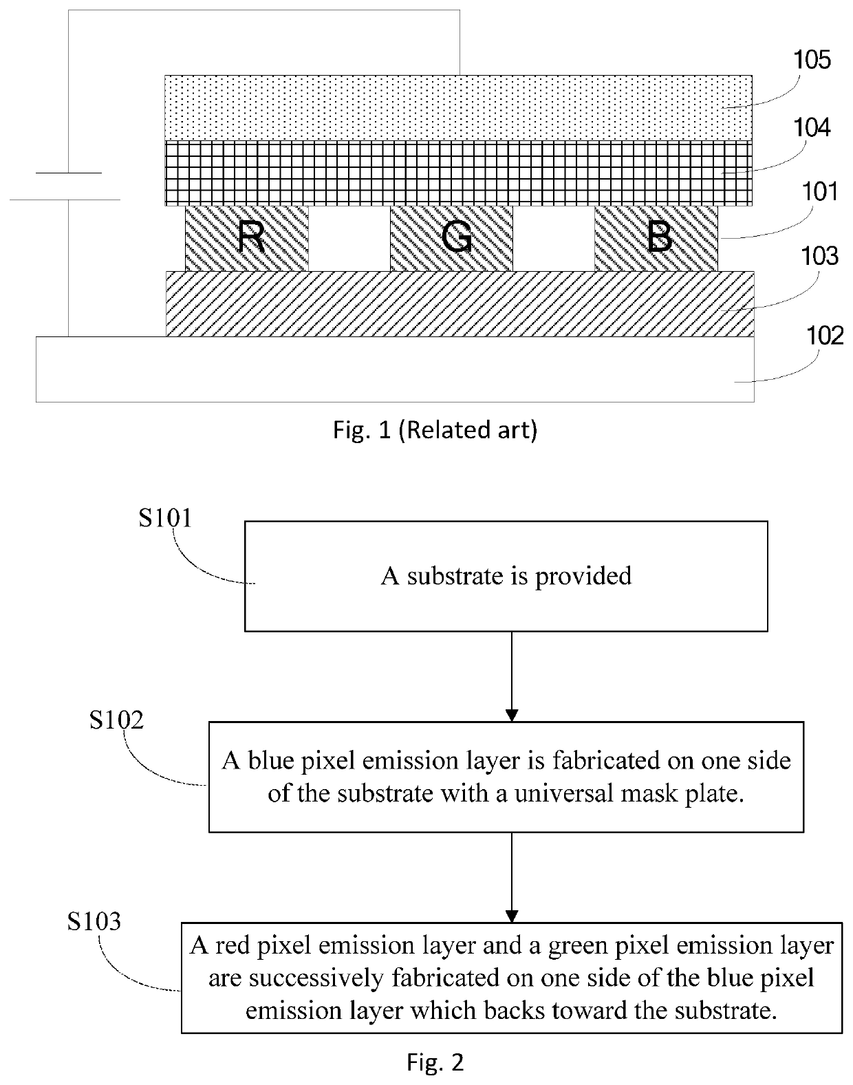
[0013]FIG. 2 is a flow diagram of a fabrication method of an organic electroluminescent device according to an embodiment of the present disclosure. The method includes block S101, block S102, and block S103.

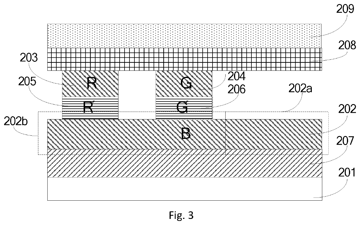
[0014]At block S101, a substrate is provided. Accompanied by FIG. 3, FIG. 3 is a schematic diagram of an organic electroluminescent device according to an embodiment of the present disclosure. A substrate 201 is configured to be an anode of the organic electroluminescent device. The property of material for the substrate 201 requires high work function and excellent transparency such as indium tin oxide (ITO), polyester thin film, and plastics.

[0015]At block S102, a blue pixel emission layer is fabricated on one side of the substrate with a universal mask plate. Accompanied by FIG. 3, material for the blue pixel emission layer 202 includes body material and a doping. The body material has a capacity of hole transport; that is, the hole mobility of the body material is greater th...


PUM

PropertyMeasurementUnit
wavelengthaaaaaaaaaa

Abstract

A fabrication method of an organic electroluminescent device includes: providing a substrate configured to an anode of the device; fabricating a blue pixel emission layer on one side of the substrate with a universal mask plate; and fabricating a red pixel emission layer and a green emission layer successively on one side of the blue pixel emission layer which backs toward the substrate. The blue pixel emission layer includes an effective emission area and a non-effective emission area. The red pixel emission layer and the green pixel emission layer both are the same layer and arranged on the non-effective emission area. The present disclosure can reduce equipment expenditure in fabricating the emission layers and the complexities of technology.

Description

BACKGROUND1. Field of the Disclosure[0001]The present disclosure relates to the technical field of display, and more particularly, to an organic electroluminescent device and a fabrication method of the organic electroluminescent device.2. Description of the Related Art[0002]With advantages of spontaneous light emission, low driving voltage, highly effective illumination, short response time, etc., organic light-emitting diode (OLED) display devices are regarded as enormous potential for industrial development.[0003]FIG. 1 is a schematic diagram of a conventional organic electroluminescent device. The organic electroluminescent device of the related art includes a substrate 102, a hole transport layer 103, an emission layer 101, an electron transport layer 104, and a metallic cathode layer 105. The emission layer 101 is formed by a red pixel emission layer (R), a green pixel emission layer (G), and a blue pixel emission layer (B). The red pixel emission layer (R), the green pixel em...

Claims


Application Information

Patent Timeline
Patent Type & Authority Patents(United States)
IPC IPC(8): H01L51/56H01L27/32H01L51/52
CPCH01L27/3218H01L51/56H01L27/3211H01L51/5265H10K59/35H10K50/852H10K71/00H10K59/353
Inventor PEI, LEICHI, MINGMING
Owner WUHAN CHINA STAR OPTOELECTRONICS SEMICON DISPLAY TECH CO LTD
Why Eureka
Try Eureka