Strontium tetraborate as optical coating material

a technology of strontium tetraborate and optical coating, which is applied in the field of optical coating materials, can solve the problems of inability to stabilize as time goes by, difficulty in generating srb4o7 layer mechanical properties, and difficulty in generating srb4o7 layer, etc., to facilitate the generation of improved frequency conversion crystals, slow or stop diffusion

Active Publication Date: 2021-02-16
KLA CORP
View PDF39 Cites 5 Cited by
  • Summary
  • Abstract
  • Description
  • Claims
  • Application Information

AI Technical Summary

Benefits of technology

[0012]Strontium tetraborate exhibits optical and mechanical properties that make it uniquely qualified for use as an optical coating material in semiconductor inspection and metrology systems that utilize deep ultraviolet (DUV) and vacuum ultraviolet (VUV) light in the range between 100 nm and 300 nm, and may also be useful in other systems that utilize visible light or infrared (IR) radiation (e.g., optical lithographic systems or IR camera systems). Although the published transparency range of SrB4O7 is 130 nm to 3200 nm, the present inventors believe a SrB4O7 optical layer may be suitably transparent to light having wavelengths a little shorter than 130 nm, perhaps to 120-125 nm. The refractive indices of SrB4O7 are high compared with conventional optical coating materials such as MgF2. The optical damage threshold is very high (14.7 GW / cm2) compared with other coating materials such as MgF2. The microhardness of SrB4O7 is also high (1750 kg / mm2 in the x direction, 1460 kg / mm2 in the y direction and 1350 kg / mm2 in the z direction). The high optical damage threshold and microhardness allow SrB4O7 coatings to withstand the extreme conditions occurring within a semiconductor inspection and metrology system, especially systems that utilize DUV and VUV radiation. That is, the DUV and VUV lasers utilized in semiconductor inspection and metrology systems often have high power levels from several milli-watts (mW) to several watts (W) or more, and high photon energy (for example 6.5 eV at 193 nm and 4.66 eV at 266 nm). Pulsed lasers may have short pulse lengths (ns or less) and high repetition rates (tens of kHz or greater). By providing such systems with optical components having an optical coating layer consisting essentially of strontium tetraborate (i.e., at least 99% of the layer is SrB4O7) that is operably disposed on the component's substrate structure, the optical and / or mechanical properties of SrB4O7 extend the operating lifetime of the optical components, thereby allowing the systems to achieve substantially longer uninterrupted operating periods and substantially reduced overall operating costs than conventional systems.
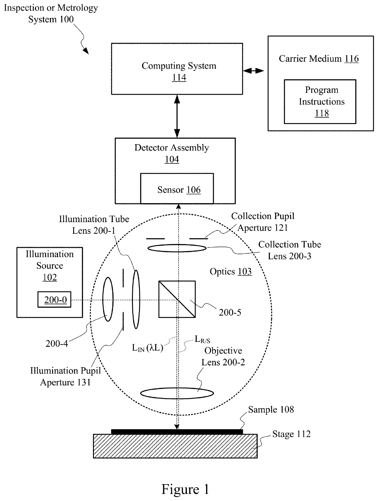
[0013]In accordance with an exemplary practical embodiment, the present invention is directed to a DUV or VUV semiconductor inspection / metrology system including an illumination (light) source that is configured to generate incident light having a wavelength in the range between 100 nm and 300 nm, and including an optical system that is configured to direct the incident light from a source to a sample, and to direct reflected / scattered light from the sample to a sensor. According to an aspect of the invention, at least one optical component utilized in at least one of the illumination (light) source and the optical system includes a strontium tetraborate (SrB4O7) optical coating layer that is operably disposed on at least one surface the component's core substrate structure. For example, the strontium tetraborate optical coating layer is formed over a light-receiving (top) surface of the component's substrate such that incident light or reflected / scattered light that is directed toward the light-receiving surface necessarily passes through the strontium tetraborate optical coating layer before reaching the light-receiving surface. In alternative embodiments, the optical component can be of any type utilized in the illumination source or optical system of an inspection and metrology system, including reflection and transmission optical components (e.g., mirrors, lenses, windows, beam splitters, polarizers and prisms), plasma arc lamps, frequency conversion crystals and laser cavities. By providing one or more SrB4O7 optical coating layers on at least one of these optical components, the mechanical properties of SrB4O7 provide enhanced protection of underlying optical materials (i.e., as compared to a similar optical component utilizing only conventional optical coating materials), thereby increasing the optical component's effective lifetime, which in turn increases the length of uninterrupted operating periods and reduces the overall operating costs of the host DUV / VUV semiconductor inspection / metrology system.
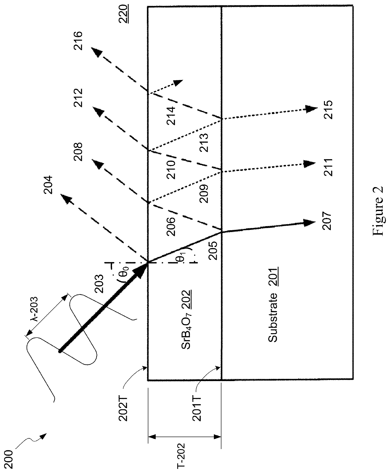
[0014]In some single layer embodiments the SrB4O7 optical coating layer is formed directly on a top (light receiving) surface of an optical component's base material (generally referred to as a substrate). In these embodiments the optical component's reflectivity (i.e., the amount of incident light that is reflected) is adjustable by way of adjusting the thickness of the SrB4O7 optical coating layer. In one embodiment, the SrB4O7 optical coating layer is formed in a manner that minimizes the reflected amount of DUV / VUV light away from the top surface of the substrate (e.g., by forming the SrB4O7 optical coating layer with a thickness equal to one-half of the wavelength of the light in the optical coating layer of the received light, whereby destructive interference occurs for the reflected beams when light is incident on the coated optics, and thus the reflectance of the component is greatly reduced at, at least, a wavelength of interest). In another embodiment, the SrB4O7 optical coating layer is formed in a manner that maximizes the reflected amount of DUV / VUV light away from the top surface of the substrate. To facilitate both increased or decreased reflectivity in DUV or VUV semiconductor inspection and metrology systems, the SrB4O7 optical coating layer is formed with a thickness in a range between 30 nm and 200 nm. Utilizing a single SrB4O7 optical coating layer takes advantage of both the optical and mechanical properties of SrB4O7, thereby providing the extending component lifetime benefits mentioned above while minimizing component production costs (i.e., by utilizing the optical properties of SrB4O7 to provide the desired optical coating characteristics (e.g., reflectivity), thereby avoiding the additional production costs that would be associated with the formation of one or more additional optical material layers that would otherwise be needed to provide the desired optical coating characteristics).
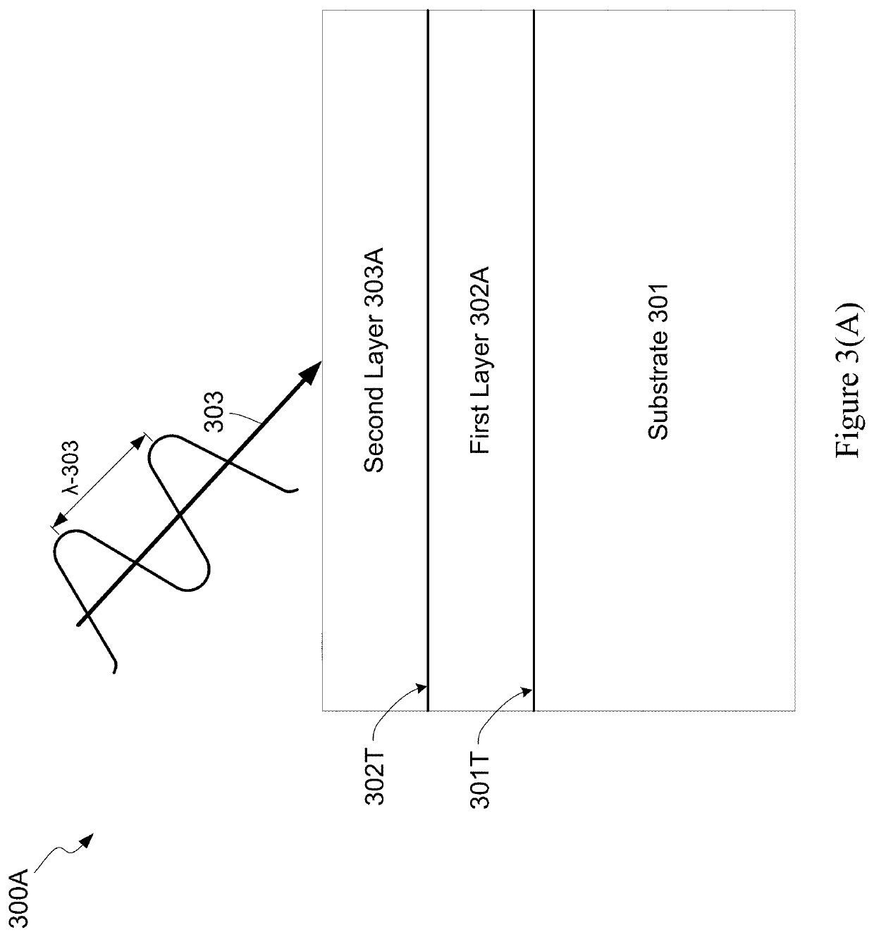
[0015]In other embodiments optical components include multiple optical coating layers formed on the optical component's substrate, where at least one layer of the multi-layer coating consists essentially of SrB4O7. In some specific embodiments the SrB4O7 optical coating layer forms the outermost coating layer of the component's multi-layer optical coating structure (i.e., such that one or more conventional (second) optical coating layers are formed between the SrB4O7 optical coating layer and the top surface of the substrate). In some embodiments, the one or more conventional optical material layers comprise one or more conventional optical coating materials such as hafnium oxide, aluminum oxide, silicon dioxide, aluminum fluoride and / or magnesium fluoride. This arrangement may be utilized to prolong the effective lifetime of an optical component by utilizing the enhanced mechanical properties of the SrB4O7 layer to shield the underlying conventional optical coating layer(s). In other embodiments, one or more conventional (third) optical material layers may be formed over the SrB4O7 optical coating layer to facilitate beneficial optical qualities that might be gained from this arrangement, while utilizing the enhanced mechanical properties of the SrB4O7 layer to protect underlying conventional (second) optical material layers and / or the substrate. In yet other embodiments, the SrB4O7 optical coating layer is formed directly on the top surface of the substrate, and one or more conventional (second) optical material layer(s) are formed over the (SrB4O7) optical material layer, thereby utilizing the enhanced mechanical properties of the SrB4O7 layer to protect only the substrate.
[0016]In some embodiments the SrB4O7 layer covers multiple (e.g., top and opposing bottom) surfaces of a substrate structure, and in other embodiments the SrB4O7 layer extends over all outer peripheral substrate surfaces to form a continuous encapsulating structure that entirely surrounds the substrate structure. In some embodiments, an inspection or metrology system includes a laser in its light source, the laser including a frequency conversion crystal configured to generate a deep UV wavelength, such as a wavelength shorter than 300 nm. The substrate of such frequency conversion crystals often comprises a hygroscopic non-linear optical material such as cesium lithium borate (CLBO) or cesium borate (CBO). The continuous SrB4O7 encapsulating structure configuration facilitates the generation of improved frequency conversion crystals by utilizing the enhanced mechanical properties of the SrB4O7 layer to slow or stop the diffusion of water and / or oxygen into the hygroscopic non-linear optical material, thus enabling the crystal to be stored, shipped and operated in a higher humidity environment than would otherwise be possible. In some embodiments desirable optical characteristics may be achieved using optional conventional optical coating material layer(s) that are either disposed inside or outside of the continuous SrB4O7 encapsulating structure.
[0017]Semiconductor inspection tools must operate at high speed in order to inspect a large fraction, or even 100%, of the area of a photomask, reticle, or wafer, in a short period of time. For example, inspection time may be one hour or less for inspection during production or, at most, a few hours for R&D or troubleshooting. In order to inspect so quickly, inspection tools use pixel or spot sizes larger than the dimensions of the defect or particle of interest, and detect just a small change in signal caused by a defect or particle. High speed inspection is most commonly performed in production using inspection tools operating with ultraviolet (UV) light. High precision metrology tools are required for accurately measuring the dimensions of small features down to a few nanometers or less on semiconductor wafers. Metrology processes are performed on wafers at various points in a semiconductor manufacturing process to measure a variety of characteristics of the wafers such as a width of a patterned structure on the wafer, a thickness of a film formed on the wafer, and an overlay offset of patterned structures on one layer of the wafer with respect to patterned structures on another layer of the wafer. These measurements are used to facilitate process controls and / or yield efficiencies in the manufacture of semiconductor dies. High-speed inspection and metrology require high light levels and a stable signal. Optical coatings that reduce the reflection losses of transmissive optics and increase the reflection of reflective optics increase the light available at the sensor and thus allow for higher sensitivity and higher speed. Coatings that do not degrade, or degrade more slowly than existing coatings, can result in a more stable signal making it easier to detect small changes in signal. Such coatings also can reduce the operating cost of an inspection or metrology tool by reducing the frequency of replacement of optical components.

Problems solved by technology

Optical coatings in the DUV (˜200 nm to 280 nm) and VUV (˜100 nm to 200 nm) spectral ranges are challenging.
However, MgF2 coatings, which are necessarily amorphous, may not be stable as time goes by.

Method used


Image

  • Strontium tetraborate as optical coating material
  • Strontium tetraborate as optical coating material
  • Strontium tetraborate as optical coating material

Examples


Embodiment Construction

[0026]Although the claimed subject matter will be described in terms of certain embodiments, other embodiments, including embodiments that do not provide all of the benefits and features set forth herein, are also within the scope of this disclosure. Various structural, logical, process step, and electronic changes may be made without departing from the scope of the disclosure. Accordingly, the scope of the disclosure is defined only by reference to the appended claims.

[0027]The following description is presented to enable one of ordinary skill in the art to make and use the disclosure as provided in the context of a particular application and its requirements. As used herein, directional terms such as “top,”“bottom,”“over,”“under,”“upper,”“upward,”“lower,”“down,” and “downward” are intended to provide relative positions for purposes of description and are not intended to designate an absolute frame of reference. Various modifications to the preferred embodiment will be apparent to ...


PUM

PropertyMeasurementUnit
wavelengthaaaaaaaaaa
thicknessaaaaaaaaaa

Abstract

Strontium tetraborate is used as an optical coating material for optical components utilized in semiconductor inspection and metrology systems to take advantage of its high refractive indices, high optical damage threshold and high microhardness in comparison to conventional optical materials. At least one layer of strontium tetraborate is formed on the light receiving surface of an optical component's substrate such that its thickness serves to increase or decrease the reflectance of the optical component. One or multiple additional coating layers may be placed on top of or below the strontium tetraborate layer, with the additional coating layers consisting of conventional optical materials. The thicknesses of the additional layers may be selected to achieve a desired reflectance of the optical component at specific wavelengths. The coated optical component is used in an illumination source or optical system utilized in a semiconductor inspection system, a metrology system or a lithography system.

Description

RELATED APPLICATIONS[0001]This application claims priority from U.S. Provisional Patent Application No. 62 / 845,496, entitled “STRONTIUM TETRABORATE AS OPTICAL COATING MATERIAL”, which was filed on May 9, 2019, and is incorporated by reference herein. This application also claims priority from U.S. Provisional Patent Application No. 62 / 913,643, entitled “STRONTIUM TETRABORATE AS OPTICAL COATING MATERIAL”, which was filed on Oct. 10, 2019, and is incorporated by reference herein.FIELD OF THE DISCLOSURE[0002]The present disclosure relates generally to systems of a type suitable for use in semiconductor manufacturing (e.g., to inspect and / or measure photomasks, reticles, and semiconductor wafers). In particular, the disclosure relates to optical coating materials for optical components (e.g., mirrors, lenses, prisms and lasers) implemented in metrology and inspection systems that utilize infrared, visible light, deep ultraviolet (DUV) and vacuum ultraviolet (VUV) radiation.BACKGROUND OF...

Claims


Application Information

Patent Timeline
Patent Type & Authority Patents(United States)
IPC IPC(8): G03F1/36G03F7/20G01N21/95G02F1/35G02F1/355G02B21/00G02B5/28G02B21/06G01N21/33G02B21/16H01L21/66
CPCG01N21/9501G01N21/33G02B5/285G02B21/0016G02B21/06G02B21/16G02F1/353G02F1/3551G01N2201/06113H01L22/12C23C14/067C23C14/0694C23C14/10C23C14/30G02B1/115G02B1/18G02B5/283G01N2021/95676G01N21/8806G01N21/55G01B11/24B05D5/06C09D1/00C09D5/004G01N2201/068
Inventor CHUANG, YUNG-HO ALEXXIAO-LI, YINYINGLOGINOVA, ELENAFIELDEN, JOHN
Owner KLA CORP
Why Eureka
Try Eureka