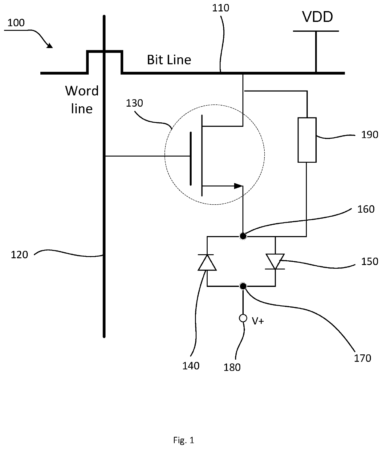
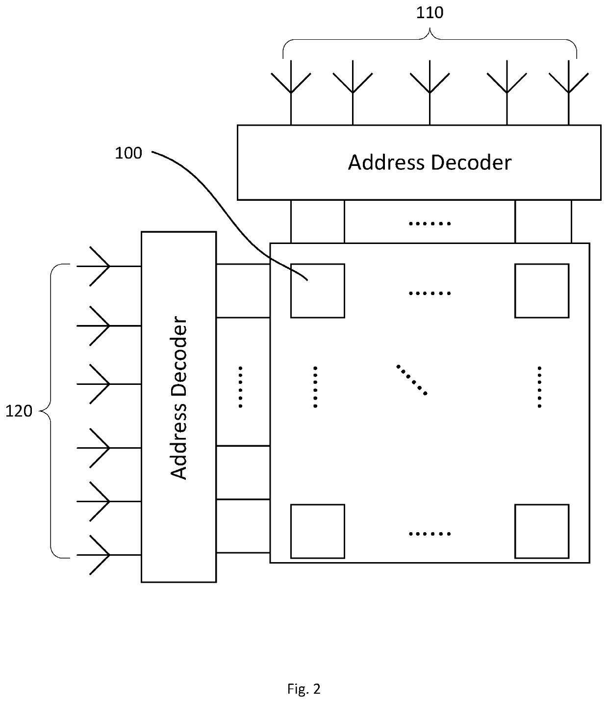
Dynamic random access memory (DRAM) cell, DRAM device and storage method
a random access memory and dynamic technology, applied in static storage, information storage, digital storage, etc., can solve the problems of capacitor discharge, capacitor leakage, energy consumption of the system, etc., and achieve the effect of improving the data transmission capability of the dram device and reducing the power consumption of the dram cell
- Summary
- Abstract
- Description
- Claims
- Application Information
AI Technical Summary
Benefits of technology
Problems solved by technology
Method used
Image

Examples
Embodiment Construction
[0047]Briefly described below are merely certain exemplary embodiments. As will be recognized by those skilled in the art, these embodiments disclosed herein may be modified in various manners without departing from the spirit or scope of the disclosure. Accordingly, the accompanying drawings and description are to be regarded as intrinsically exemplary rather than limiting.
[0048]In this disclosure, the directional and spatial terms “central,”“longitudinal,”“transverse,”“lengthwise,”“widthwise,”“thickness-wise,”“upper,”“lower,”“front,”“rear,”“left,”“right,”“vertical,”“horizontal,”“top,”“bottom,”“inner,”“outer,”“clockwise,”“counterclockwise,”“axial,”“radial,”“circumferential,” etc., are meant to be used with respect to the configurations shown in the figures. They are intended merely to facilitate and simplify the explanation of the disclosure and do not indicate or imply the stated components or elements have to assume, or be constructed or operated in, particular orientations. Ther...
PUM
 Abstract
Description
Claims
Application Information