Systems and methods for providing approximate electronic-structure models from calculated band structure data

a band structure and electronic structure technology, applied in the field of simulation of electronic devices, can solve the problems of inability to obtain reliable experimental data for such parameters for relevant device geometries, inability to construct accurate descriptions of confined devices, and inability to use effective mass and non-parabolicity parameters determined from bulk systems

Active Publication Date: 2021-06-01
SYNOPSYS INC
View PDF4 Cites 0 Cited by
  • Summary
  • Abstract
  • Description
  • Claims
  • Application Information

AI Technical Summary

Benefits of technology

[0012]The implementation of methods according to this aspect enables the identification of the interleaved band ladders of confined nanodevices and therefore, a more precise band structure for TCAD tools simulation may be obtained. Additionally, the method provides an accurate description of the confined nanodevice around the band minimum. By using this method, a simulation as fast as one performed with TCAD tools and as accurate as one performed with DFT simulations may be achieved.
[0020]The implementation of such systems provides robust and automatized procedures for extracting effective mass models from atomic-scale modeling, which may be used to simulate band structure data.

Problems solved by technology

Therefore, the values of the effective mass and non-parabolicity parameters determined from a bulk system, cannot be used to construct an accurate description of the confined device.
It can be very difficult, costly, and sometimes impossible, to obtain reliable experimental data for such parameters for relevant device geometries, e.g., a confined nanodevice.
However, it is not possible to solve the Quantum Mechanical equations exactly, and so a number of different approximations exist.
For complex nanoscale devices, the calculated band structure data can be very complex, and it can be difficult to extract an effective mass description as needed for the TCAD tools.

Method used


Image

  • Systems and methods for providing approximate electronic-structure models from calculated band structure data
  • Systems and methods for providing approximate electronic-structure models from calculated band structure data
  • Systems and methods for providing approximate electronic-structure models from calculated band structure data

Examples


Embodiment Construction

[0037]In the following description, numerous specific details are set forth regarding the systems and methods of the disclosed subject matter and the environment in which such systems and methods may operate, etc., in order to provide a thorough understanding of the disclosed subject matter. It will be apparent to one skilled in the art, however, that the disclosed subject matter may be practiced without such specific details, and that certain features, which are well known in the art, are not described in detail in order to avoid complication of the disclosed subject matter. In addition, it will be understood that the examples provided below are exemplary, and that it is contemplated that there are other systems and methods that are within the scope of the disclosed subject matter.

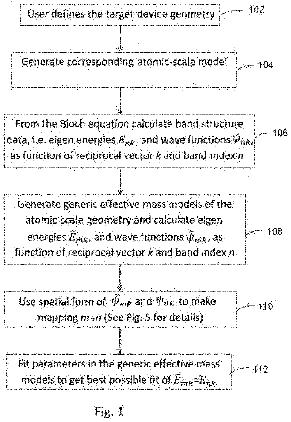
[0038]The present invention is directed to a system and method for extracting an approximate band structure model from an atomic-scale band structure calculation of a confined system. The confined systems...


PUM


Abstract

Computer-aided methods for simulating confined nanodevices are disclosed. In example implementations, atomic-scale model of the nanodevices are generated so that dimensions and materials are specified. Then, band structures which comprise wave functions and Eigen energies are calculated using First Principles Methods (FPM). Effective mass modeled which comprise wave functions and Eigen energies are generated. After that, spatial wave functions of the calculated FPM band structures are mapped to the generated effective mass band structures wave functions by considering global behavior. In response to the mapping, generated effective mass models are fitted to calculated FPM energies so that approximate electronic band structures of the confined nanodevices are modeled. Computer programs for carrying out the methods, data media and computer systems are also disclosed.

Description

CROSS-REFERENCE TO OTHER APPLICATIONS[0001]This application is a Continuation-in-Part of International Application No. PCT / EP2016 / 064628, entitled “SYSTEMS AND METHODS FOR PROVIDING APPROXIMATE ELECTRONIC STRUCTURE MODELS FROM CALCULATED BAND STRUCTURE DATA,” filed Jun. 23, 2016, which claims the benefit of U.S. Provisional Application No. 62 / 188,959, entitled “SYSTEM AND METHOD FOR PROVIDING APPROXIMATE ELECTRIC-STRUCTURE MODEL EXTRACTION FROM CALCULATED BAND STRUCTURE DATA,” filed 6 Jul. 2015, which applications are incorporated herein by reference in their entirety.BACKGROUND[0002]Technology Computer Aided Design (TCAD) tools are used for simulating electronic devices at the transistor level. A typical electronic device is a FinFET or a nanowire transistor. These devices have three terminals: source, drain and gate. The voltage (V gate) at the gate terminal controls the source-drain current (I).[0003]The purpose of the simulations is to predict the 1-V gate characteristics of dif...

Claims


Application Information

Patent Timeline
Patent Type & Authority Patents(United States)
IPC IPC(8): G06F30/367
CPCG06F30/367G06F30/36
Inventor STOKBRO, KURTPALSGAARD, MATTIAS
Owner SYNOPSYS INC
Why Eureka
Try Eureka