Vertical type MOSFET

a technology of vertical type and mosfet, which is applied in the direction of semiconductor devices, basic electric elements, electrical equipment, etc., can solve the problems of low yield and reliability, poor surface, and poor film quality of gate oxide film 8, and achieve the effect of small on-resistan

Inactive Publication Date: 2003-08-05
DENSO CORP
View PDF77 Cites 24 Cited by
  • Summary
  • Abstract
  • Description
  • Claims
  • Application Information

AI Technical Summary

Benefits of technology

It is an object of the present invention to provide a vertic...

Problems solved by technology

However, the R-MOS device has drawbacks in that the yield and the reliability are low.
The cause is that the trench groove 50 is formed by the reactive ion etching method, and therefore the flatness of the sidewall surface of the inner wall 51 is bad and produces many defects, and the film quality of the gate oxide film 8, which is formed by oxidizing the surface thereof, is bad.
Insulation inferiority of the gate oxide film, a decrease in the mobility due to the defect of the interface of the channel ...

Method used


Image

  • Vertical type MOSFET
  • Vertical type MOSFET
  • Vertical type MOSFET

Examples


fifth embodiment

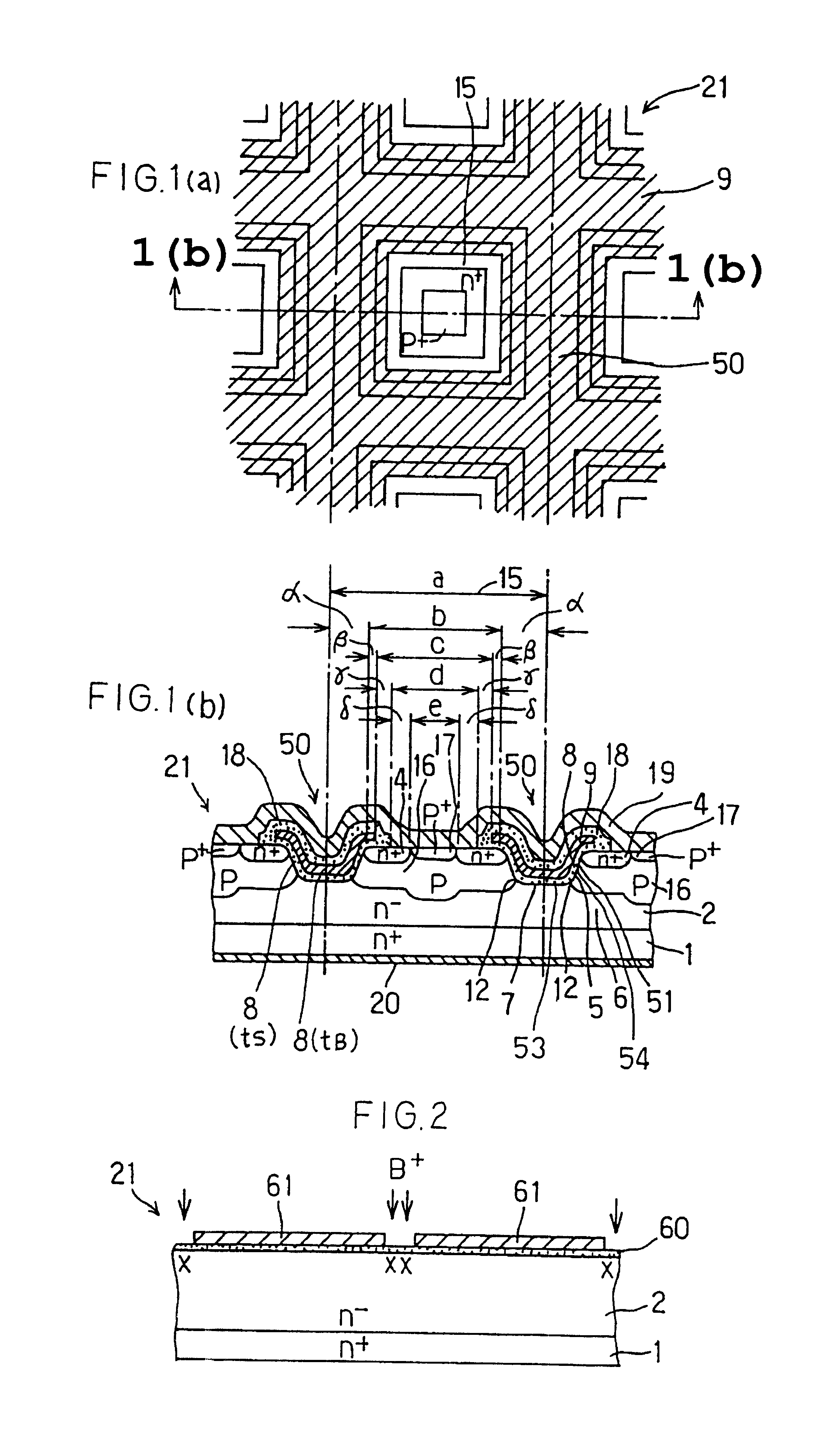
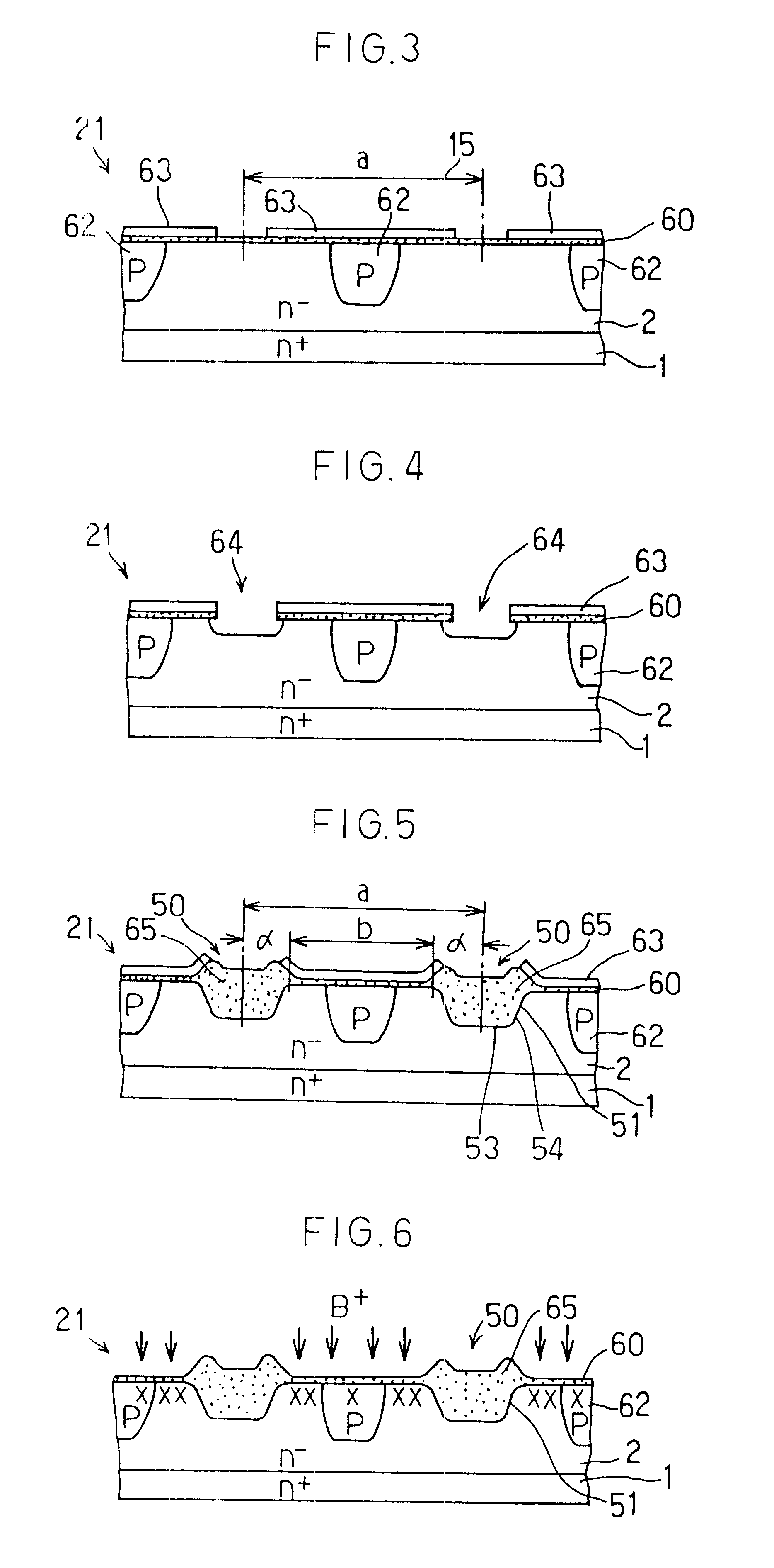
In the fifth embodiment, as shown in FIGS. 24(a) and 24(b), the wafer 21 is selected to have the index of plane of its main surface which is (101) or those near it. Thus the surface of the n.sup.- -type epitaxial layer 2 corresponding to the bottom face of the LOCOS oxide film 65 formed on the wafer 21 in the corresponding step shown in FIG. 5, that is the bottom face 53 of the U-groove 50, is parallel to the main surface, so that its index of plane is also (100).

In addition, as shown in FIG. 24(a), owing to the optimization of the directions of the sides of the rectangular unit cell 15 with respect to the plane orientation of the main surface of the wafer 21, and the optimization of the inclination angle of the side face 54 of the U-groove 50 by condition setting in the LOCOS oxidation step shown in FIG. 5, the index of plane of the side face 54 of the U-groove 50 is set to be an index of approximately (111). That is, the index of plane of the side surface 54 of the U-groove 50 aft...

sixth embodiment

Furthermore, the plane orientation of the silicon substrate 1 and the patterning shape may be selected so that the index of plane of side surface 54 of the U-groove 50 can be (110) as shown in FIGS. 25(a) and 25(b). FIG. 25(a) is a plane view of a vertical power MOSFET comprising rectangular unit cells 15 according to the present invention, and FIG. 25(b) is a cross-sectional view taken along 25(b)--25(b) in FIG. 25(a).

In the sixth embodiment, as shown in FIG. 25(a), a pattern of a rectangular unit cell 15 and a U-groove 50 of a lattice-like pattern are used, and a face direction of one side of the rectangle or the lattice is set to be , and further as shown in FIG. 25(b), in order to provide an angle of 45.0.degree. formed by the main surface of a wafer 21 and a side face 54 of the U-groove 50, the conditions in the LOCOS oxidation step shown in FIG. 5 are set. By doing so, index of planes of all of the side faces 54 of the U-groove 50 can be made (110).

Now, a manufacturing method ...

seventh embodiment

In this vertical power MOSFET 100, the same effects as that of the seventh embodiment can be obtained by integrally forming the p-type base layer 108.

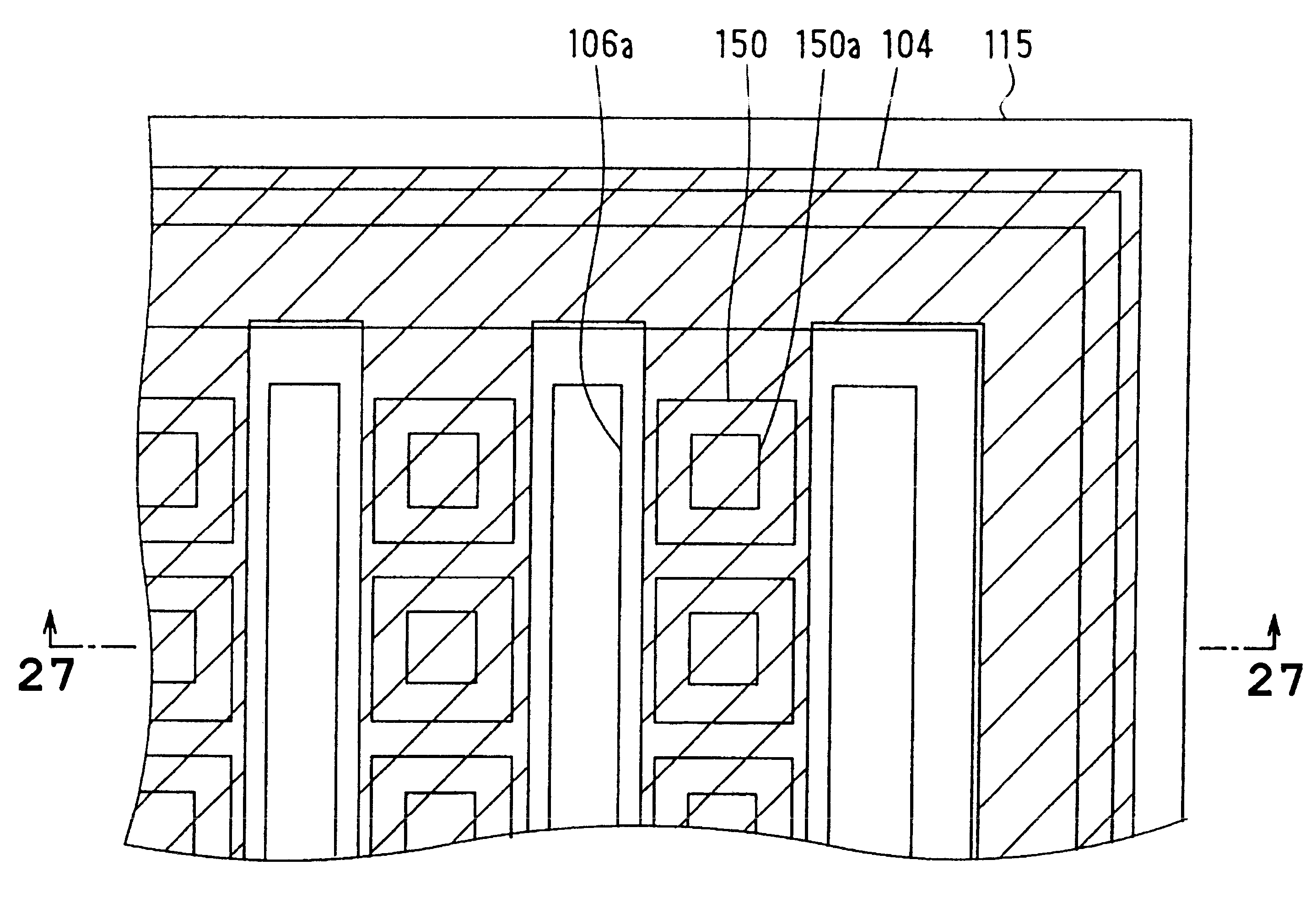
Next, a production method of a vertical power MOSFET 100 will be explained with reference to FIGS. 32(a)-32(c).

[Step Shown in FIG. 32(a)]

A wafer 121 having the same construction as that in the seventh embodiment is provided. A p-type deep-base layer 109 is formed by the same step shown in FIG. 29(a), and a thicker oxide film 115 is formed at a region to be the non-active region of the element by a LOCOS oxide method.

After that, a p-type base layer 108, an n.sup.+ -type source layer 107, and a p-type contact layer 111 are formed through with a photolithography step.

[Step Shown in FIG. 32(b)]

Next, a groove portion 160 penetrating the p-type base layer 109 and n.sup.+ -type source layer 107 is formed by etching. By doing this step, at the sidewalls of the U-grooves 150, the p-type base layer 108 is arranged between the n.sup.+ -type sourc...


PUM


Abstract

A vertical power MOSFET, which can improve a surge withstand voltage and a surge withstand voltage against a surge voltage from an inductance load L. The vertical power MOSFET has a plurality of unit cells. The unit cell is formed from a MOSFET that uses a p-type base layer at a sidewall of a rectangular U-groove as a channel portion. Each of the p-type base layer of each unit cell is connected each others Accordingly, it can restrain an impurity concentration of a corner portion (a portion positioned at a corner) of the rectangular p-type base layer from being decreased. Therefore, it can reduce the difference in distance from the end portion of the p-type base layer to the end portion of the depletion layer. As a result, it can improve the surge withstand voltage when a surge voltage is input from an inductance load L.

Description

1. Technical FieldThe present invention relates to a semiconductor device to be used as an electric power semiconductor device, especially to a vertical type MOSFET (Metal Oxide Semiconductor Field Effect Transistor), which is preferable in the case of adoption as MOSIC and the like in which an elemental article thereof or the semiconductor device fore electric power is incorporated.2. Background ArtThe vertical type power MOSFET has many features such that it has excellent frequency characteristics, has a fast switching velocity, can be driven at low electric power and the like, so that it has recently been used in many industrial fields. For example, in "Nikkei Electronics" published by Nikkei-McGraw-Hill, Inc. on May 19, 1986, pp. 165-188, it is described that the focus of development of the power MOSFET is in migrating to low voltage resistant articles and high voltage resistant articles. Further, it is described in this literature that the ON-resistance of a power MOSFET chip h...

Claims


Application Information

Patent Timeline
IPC IPC(8): H01L29/10H01L29/78H01L21/02H01L21/336H01L29/06H01L29/66H01L29/40H01L29/02H01L29/423
CPCH01L29/0696H01L29/1095H01L29/7813H01L29/4236H01L29/045
Inventor OKABE, YOSHIFUMIOZEKI, YOSHIHIKOTAKAHASHI, SHIGEKITOKURA, NORIHITO
Owner DENSO CORP
Why Eureka
Try Eureka