Organic light-emitting diode (OLED) display device including sensor disposed in groove of base substrate
a technology of organic light-emitting diodes and display devices, which is applied in the field of display technology, can solve the problems of low integration of display devices, reducing the effective display area, and still having important defects, so as to avoid image capture blur, improve integration, and optimize the effect of process complexity caused by external leads
- Summary
- Abstract
- Description
- Claims
- Application Information
AI Technical Summary
Benefits of technology
Problems solved by technology
Method used
Image
Examples
first embodiment
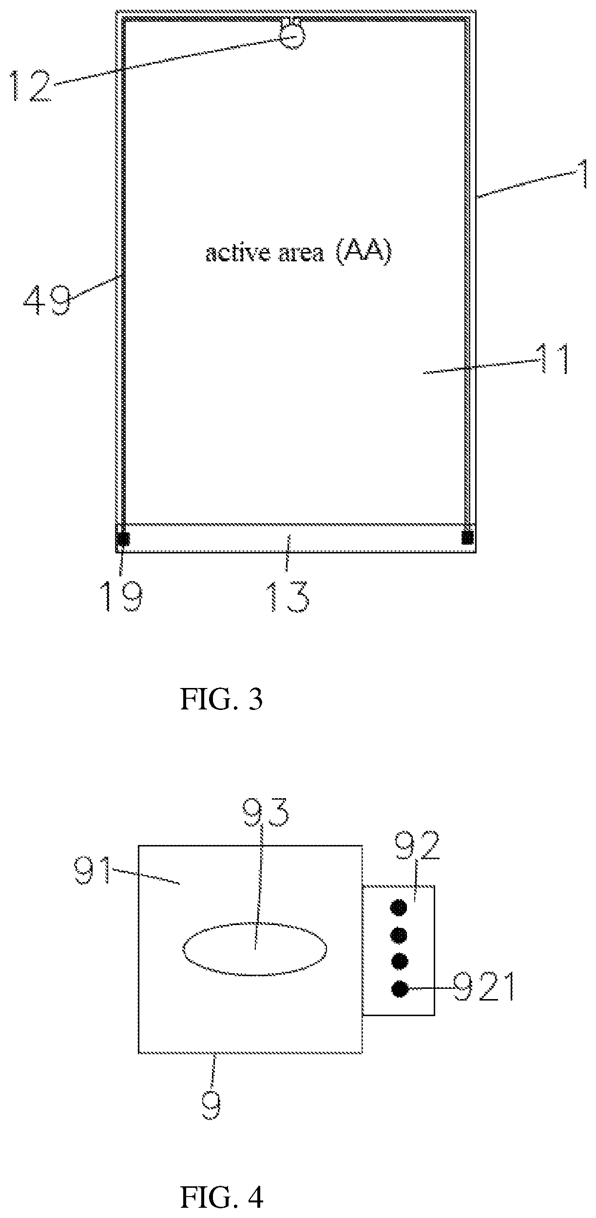
[0033]Referring to FIG. 3, an organic light-emitting diode (OLED) display device according to the present invention includes a display panel 1 and an image capturing assembly 9 disposed in the display panel 1.
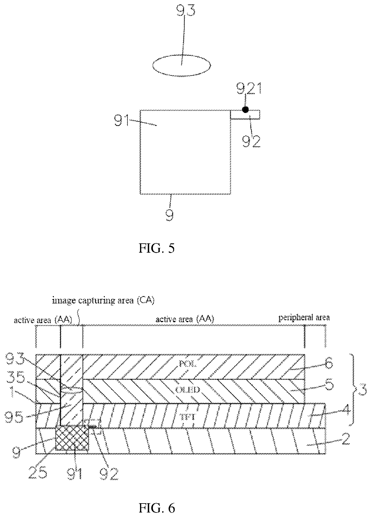
[0034]The display panel 1 includes a base substrate 2 and a display layer 3 provided on the base substrate 2.
[0035]The display layer 3 includes a thin film transistor (TFT) layer 4 disposed on the base substrate 2, an OLED functional layer 5 disposed on the TFT layer 4, a thin film encapsulation layer sequentially disposed on the OLED functional layer 5 (not shown) and polarizing layer (POL) 6.
[0036]The display panel 1 is divided into a display area 11, an image capturing area 12 located in the display area 11, and a peripheral area 13 located outside the display area 11.
[0037]As shown in FIGS. 4-5, the image capturing assembly 9 mainly includes a sensor 91, a signal module 92 electrically connected to the sensor 91 disposed on a side of an upper end of the sensor 91, and a len...
second embodiment
[0052]the present invention provides an organic light-emitting diode (OLED) display device, which improves the integration degree between the display panel and the image capturing assembly in the manufacturing process of assembling the image capturing assembly 9 in the display panel 1, by separately integrating the sensor 91 and the lens 93 of the image capturing assembly 9 into a structure of the display panell, which avoids the matching problem between the image capturing assembly 9 and the display panel 1 produced by different manufacturers to a certain extent. In addition, the base substrate 2 adopts a groove design in the image capturing area 12 to build in the sensor 91 on the substrate, avoiding problems such as image capturing blur caused by poor light transmittance of the polyimide (PI) substrate on the image capturing assembly 9 of a conventional design. Further, the source / drain metal layer in the TFT layer 4 is provided with an image capturing signal transmission line el...
PUM
| Property | Measurement | Unit |
|---|---|---|
| area | aaaaa | aaaaa |
| height | aaaaa | aaaaa |
| depth | aaaaa | aaaaa |
Abstract
Description
Claims
Application Information


