Polyimide cover substrate
a polyimide and substrate technology, applied in the field of polyimide cover substrates, can solve problems such as surface cracking problems in the evaluation of flexural properties or impact resistance, and achieve the effects of high flexural properties and impact resistance, superior solvent resistance, optical properties and scratch resistance, and low water vapor transmission ra
- Summary
- Abstract
- Description
- Claims
- Application Information
AI Technical Summary
Benefits of technology
Problems solved by technology
Method used
Image
Examples
preparation example 1
1-1: Preparation of Polyimide Powder
[0098]While a 1 L reactor equipped with a stirrer, a nitrogen inlet tube, a dropping funnel, a temperature controller and a condenser was purged with nitrogen, 832 g of N,N-dimethylacetamide (DMAc) was placed, the temperature of the reactor was adjusted to 25° C., 64.046 g (0.2 mol) of bistrifluoromethyl benzidine (TFDB) was dissolved, and this solution was maintained at 25° C. 31.09 g (0.07 mol) of 2,2-bis(3,4-dicarboxyphenyl)hexafluoropropane dianhydride (6FDA) and 8.83 g (0.03 mol) of biphenyl tetracarboxylic dianhydride (BPDA) were added, and dissolved and reacted with stirring for a predetermined period of time. The temperature of the solution was maintained at 25° C. 20.302 g (0.1 mol) of terephthaloyl chloride (TPC) was added, thus obtaining a polyamic acid solution having a solid content of 13 wt %. The polyamic acid solution was added with 25.6 g of pyridine and 33.1 g of acetic anhydride, stirred for 30 min, further stirred at 70° C. for...
example 1
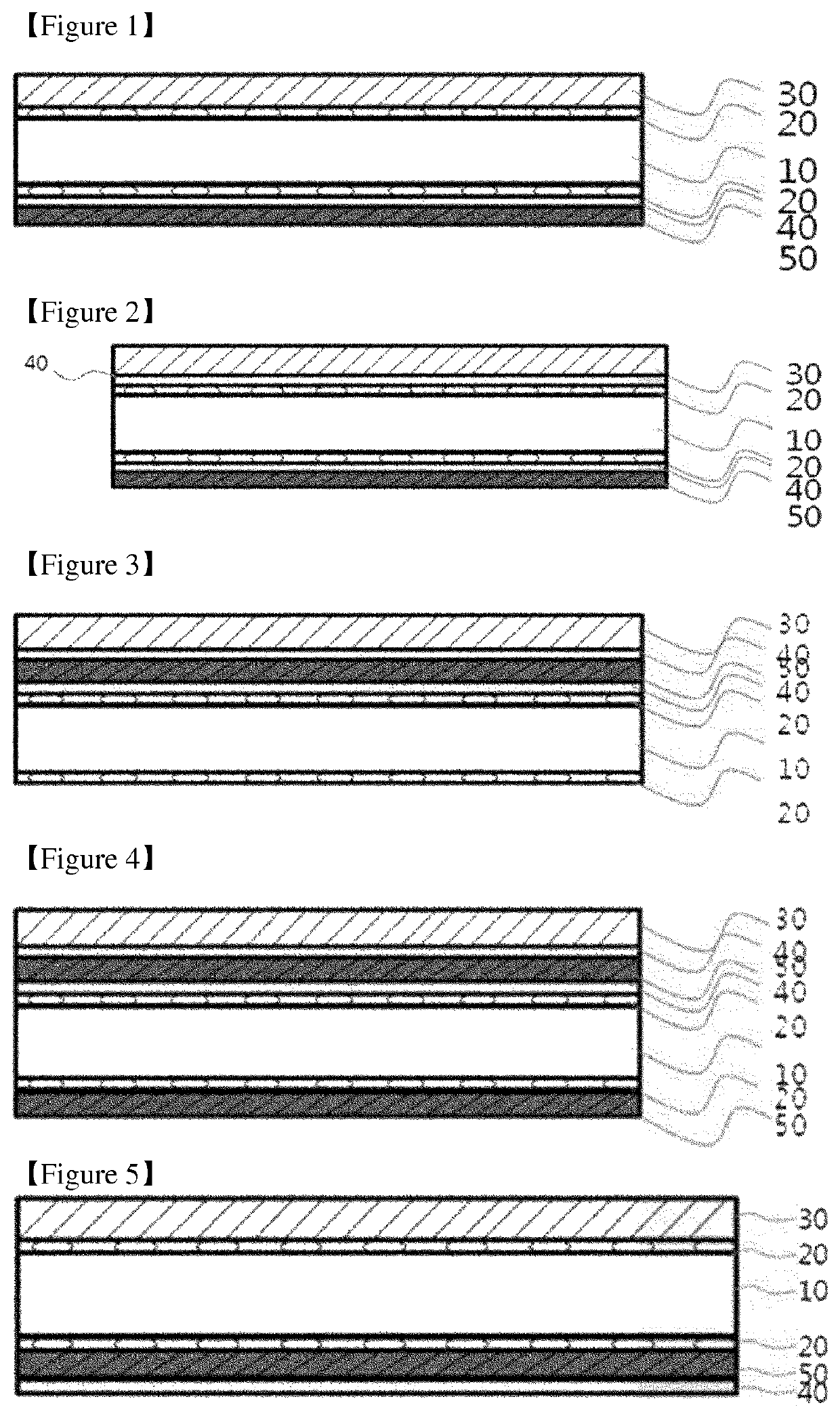
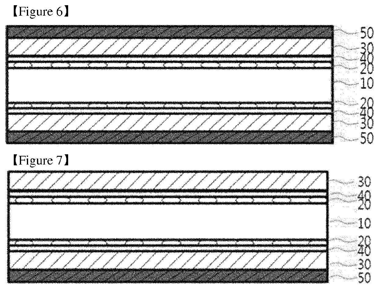
[0104]Silicon oxide layers were formed in the same manner as in Comparative Example 2 on both surfaces of the colorless transparent polyimide film, and the acrylate-containing polyisocyanate solution used in Comparative Example 3 was applied, dried and cured in the same manner as in Comparative Example 3 on one of the silicon oxide layers, thus forming a hard coating layer 10 μm thick. Then, ITO was deposited on the other silicon oxide layer opposite the hard coating layer using a sputter, thus forming a transparent electrode layer. 10 g of a urethane acrylate compound (KLH-100, NATOCO) having a weight average molecular weight of 8,000 g / mol and represented by Chemical Formula 1 in which R is a hexyl group was dissolved in 10 g of methylethylketone (MEK), and then the resulting solution having the dissolved urethane acrylate compound was applied on the transparent electrode layer by means of a bar coater and then dried at 80° C., thus obtaining a coating film 10 μm thick. Then, two ...
example 2
[0105]In the same manner as in Example 1, silicon oxide layers were formed on both surfaces of the polyimide film, and transparent electrode layers were formed on outer surfaces of the silicon oxide layers. Also, a hard coating layer was formed on one of the transparent electrode layers, and a device protection layer was formed on the other transparent electrode layer opposite the hard coating layer, thereby manufacturing a polyimide cover substrate (FIG. 2) including the device protection layer, the transparent electrode layer, the silicon oxide layer, the polyimide film, the silicon oxide layer, the transparent electrode layer and the hard coating layer, which were sequentially stacked.
PUM
| Property | Measurement | Unit |
|---|---|---|
| thickness | aaaaa | aaaaa |
| thickness | aaaaa | aaaaa |
| transmittance | aaaaa | aaaaa |
Abstract
Description
Claims
Application Information
 - R&D
- Intellectual Property
- Life Sciences
- Materials
- Tech Scout
- Unparalleled Data Quality
- Higher Quality Content
- 60% Fewer Hallucinations
Browse by: Latest US Patents, China's latest patents, Technical Efficacy Thesaurus, Application Domain, Technology Topic, Popular Technical Reports.
© 2025 PatSnap. All rights reserved.Legal|Privacy policy|Modern Slavery Act Transparency Statement|Sitemap|About US| Contact US: help@patsnap.com


