Pulse current generation circuit for neural stimulation, charge compensation circuit and method, and implantable electrical retina stimulator
a current generation circuit and neural stimulation technology, applied in the field of neural stimulation, can solve the problems of rarely good stimulation effect, inability to effectively stimulate retinal bipolar cells slightly away from the retina surface, and the stimulating current generated for neural stimulation may not guarantee that the charge amount during one stimulation period falls within a safe range. , to achieve the effect of effective stimulation effect, improving the efficiency of charge balance, and ensuring safety and reliability of neural stimulation
- Summary
- Abstract
- Description
- Claims
- Application Information
AI Technical Summary
Benefits of technology
Problems solved by technology
Method used
Image
Examples
first embodiment
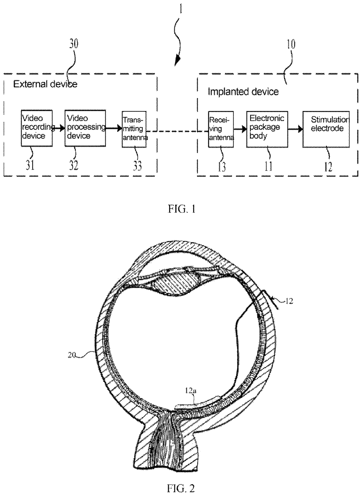
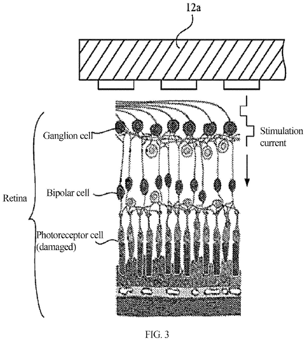
[0043]FIG. 1 is a structural schematic diagram showing an implantable electrical retina stimulator according to a first embodiment of the present invention. FIG. 2 is a schematic diagram showing the implantation of a stimulation electrode structure of the implantable electrical retina stimulator according to the first embodiment of the present invention into an eyeball. FIG. 3 is a partial schematic diagram showing the attachment of the stimulation electrode structure (a stimulation end) shown in FIG. 2 to the retina in the eyeball.
[0044]In the present embodiment, as shown in FIG. 1, the implantable electrical retina stimulator (sometimes referred to as an “artificial retina” or “artificial retina system”) 1 may include a part implanted into human body, i.e., an implanted device 10, and apart outside the body, i.e., an external device 30. In the implantable electrical retina stimulator according to the present embodiment, the implanted device 10 and the external device 30 may be cou...
second embodiment
[0090]FIG. 9 is a schematic diagram showing a circuit structure of a pulse current generation circuit according to the second embodiment of the present invention. FIG. 10 is a schematic diagram showing a circuit structure of a charge compensation circuit according to the second embodiment of the present invention. FIG. 11 is a schematic diagram showing a compensation pulse current according to the second embodiment of the present invention. FIG. 12 is a schematic diagram showing a circuit structure of the charge compensation circuit according to the second embodiment of the present invention.
[0091]The pulse current generation circuit 200 according to the second embodiment differs from the pulse current generation circuit 100 according to the first embodiment in that besides the analogue signal receiving device 101, the analogue-to-digital converter 102, the current signal controller 103 and the current generator 104 according to the first embodiment, the charge compensation circuit ...
PUM
 Abstract
Description
Claims
Application Information


