Display device having a reflective portion covered bank sidewall

a technology of a display device and a sidewall is applied in the field of display devices displaying images, which can solve the problems of color mixture and light loss caused by viewing angles, and the problem of more serious problems, so as to achieve the effect of preventing light loss as well as color mixture and improving light efficiency

Active Publication Date: 2021-09-28
LG DISPLAY CO LTD
View PDF19 Cites 1 Cited by
  • Summary
  • Abstract
  • Description
  • Claims
  • Application Information

AI Technical Summary

Benefits of technology

[0007]The present disclosure has been made in view of the above problems, and an aspect of the present disclosure to provide a display device that can prevent a color mixture and light loss from occurring.
[0010]In the display device according to the present disclosure, as the reflective portion adjoining the organic light emitting layer is provided on the bank, the reflective portion may reflect light, which is emitted from the first subpixel area, toward the first subpixel area to prevent the light from entering the second subpixel area adjacent to the first subpixel area through the bank, so that light loss as well as a color mixture may be prevented from occurring, whereby light efficiency may be improved.

Problems solved by technology

On the other hand, the organic light emitting display device has a problem in that light emitted at a certain angle or more is emitted to an adjacent pixel or subjected to waveguide, whereby a color mixture and light loss caused by a viewing angle occur.
This problem occurs more seriously in case of a head mounted display (HMD) including an organic light emitting display device.

Method used


Image

  • Display device having a reflective portion covered bank sidewall
  • Display device having a reflective portion covered bank sidewall
  • Display device having a reflective portion covered bank sidewall

Examples


second embodiment

[0078]FIG. 2a is a brief cross-sectional view illustrating a display device according to the present disclosure, and FIG. 2b is a view illustrating a brief layer structure of line III-III shown in FIG. 2a.

[0079]Referring to FIG. 2a, in the display device 1 according to the second embodiment of the present disclosure, the reflective portion 8 may be arranged on a top surface of the organic light emitting layer 6.

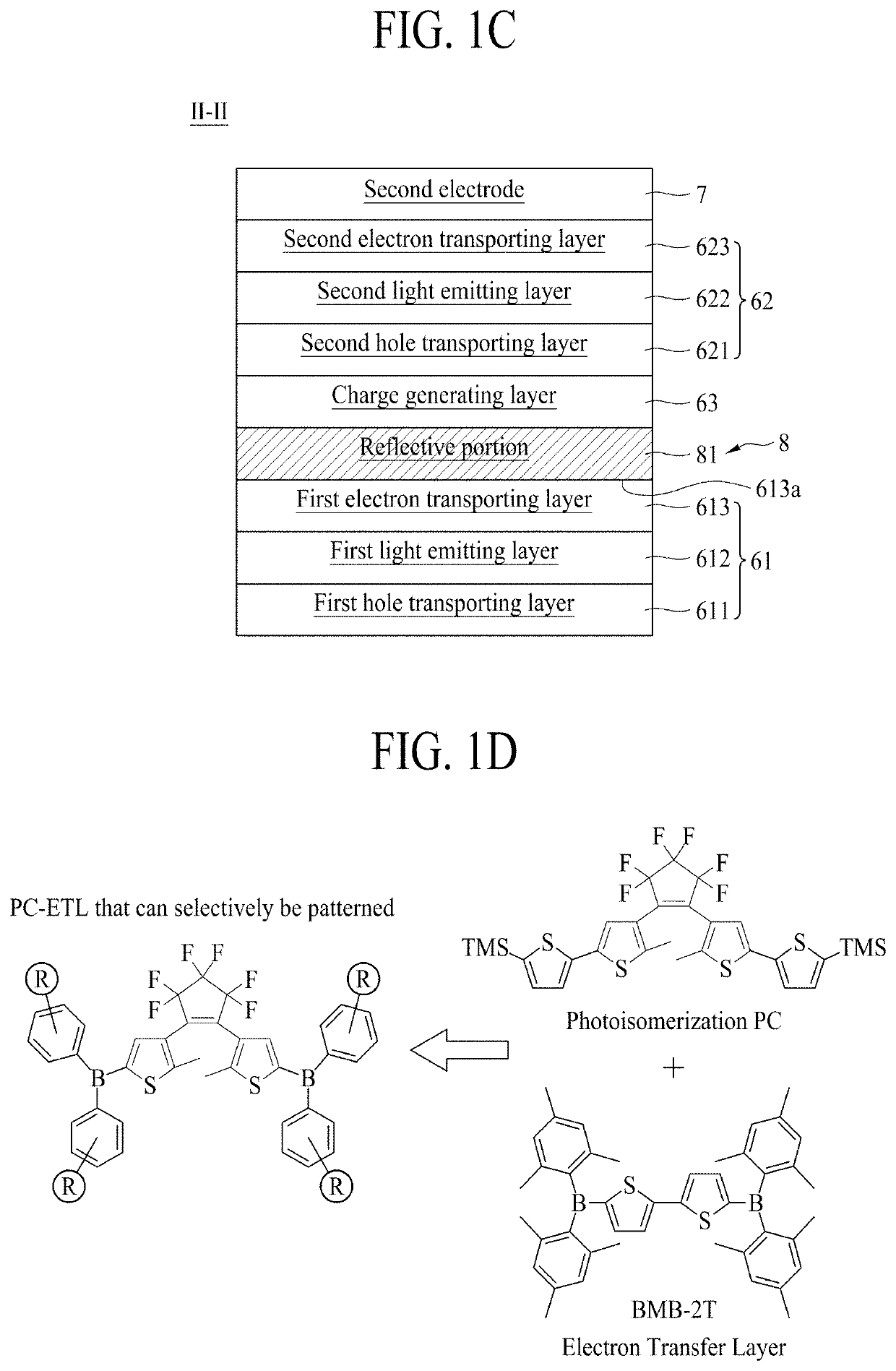
[0080]For example, as shown in FIG. 2b, if the organic light emitting layer 6 includes a hole transporting layer 631, a light emitting layer 632 and an electron transporting layer 623, the first reflective portion 81 and the second reflective portion 82 may be provided on the top surface 633a of the electron transporting layer 633. Since the hole transporting layer 631, the light emitting layer 632 and the electron transporting layer 633 respectively correspond to the first hole transporting layer 611, the first light emitting layer 612 and the first electron transporting la...

third embodiment

[0084]FIG. 3 is a brief cross-sectional view illustrating a display device according to the present disclosure.

[0085]Referring to FIG. 3, in the display device 1 according to the third embodiment of the present disclosure, the first reflective portion 81 may be extended to the top surface 51 of the bank 5. In this case, the first reflective portion 81 may be provided to cover only one side of the top surface 51 of the bank 5. Therefore, the first reflective portion 81 may be formed to be bent to partially cover the top surface 51 of the bank 5 as well as the first inclined surface 52 of the bank 5. Therefore, in the display device 1 according to the third embodiment of the present disclosure, the first reflective portion 81 may prevent the light emitted from the first subpixel area 21 from entering the bank 5 through a portion of the top surface 51 of the bank 5 as well as the first inclined surface 52 of the bank 5, whereby the color of the first subpixel area 21 may be more preven...

fourth embodiment

[0089]FIG. 4a is a brief cross-sectional view illustrating a display device according to the present disclosure, and FIG. 4b is a view illustrating a brief layer structure of line IV-IV shown in FIG. 4a.

[0090]Referring to FIG. 4a, in the display device 1 according to the fourth embodiment of the present disclosure, the reflective portion 8 may include a plurality of layers. For example, the reflective portion 8 may include a first layer 8a provided inside the organic light emitting layer 6, and a second layer 8b provided inside or on the organic light emitting layer 6 while being spaced apart from the first layer 8a.

[0091]Referring to FIG. 4b, in the display device 1 according to the fourth embodiment of the present disclosure, if the organic light emitting layer 6 includes a first stack 61, a second stack 62, and a charge generating layer 63 provided between the first stack 61 and the second stack 62, the first layer 8a may be provided on the top surface 613a of the first electro...


PUM

PropertyMeasurementUnit
areaaaaaaaaaaa
chemical structureaaaaaaaaaa
sizeaaaaaaaaaa

Abstract

A display device includes a substrate provided with a first subpixel area, and a second subpixel area adjacent to one side of the first subpixel area, a first electrode provided on the substrate, including a first sub electrode provided on the first subpixel area and a second sub electrode provided on the second subpixel area, an organic light emitting layer arranged on the first electrode, a second electrode arranged on the organic light emitting layer, a bank provided between the first sub electrode and the second sub electrode, partitioning the first subpixel area from the second subpixel area, and a reflective portion provided on the bank, adjoining the organic light emitting layer.

Description

BACKGROUNDTechnical Field[0001]The present disclosure relates to a display device displaying an image.Description of the Related Art[0002]With the advancement of the information age, the demand for a display device for displaying an image has increased with various forms. Therefore, various types of display devices such as a liquid crystal display (LCD) device, a plasma display panel (PDP) display device, and an organic light emitting display (OLED) device have been used.[0003]Among the display devices, the organic light emitting display device is a self-light emitting device, and has advantages in that a viewing angle and a contrast ratio are more excellent than those of the liquid crystal display (LCD) device. Also, since the organic light emitting display device does not require a separate backlight, it is advantageous that the organic light emitting display device is able to be thin and lightweight and has low power consumption. Furthermore, the organic light emitting display de...

Claims


Application Information

Patent Timeline
Patent Type & Authority Patents(United States)
IPC IPC(8): H01L27/32H01L51/50H01L51/52G02B27/01
CPCH01L27/3209H01L27/3246H01L51/5056H01L51/5271H01L51/5275G02B27/0172H01L2227/32H01L2251/53H10K59/122H10K50/856H10K59/32H10K59/35H10K50/16H10K50/19H10K50/00H10K50/15H10K50/858H10K59/10H10K2102/302
Inventor GONG, HYE-JIN
Owner LG DISPLAY CO LTD
Why Eureka
Try Eureka