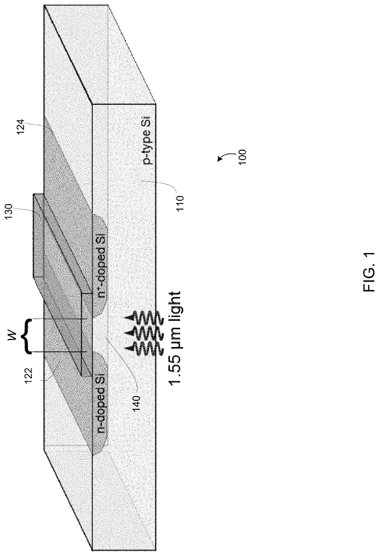
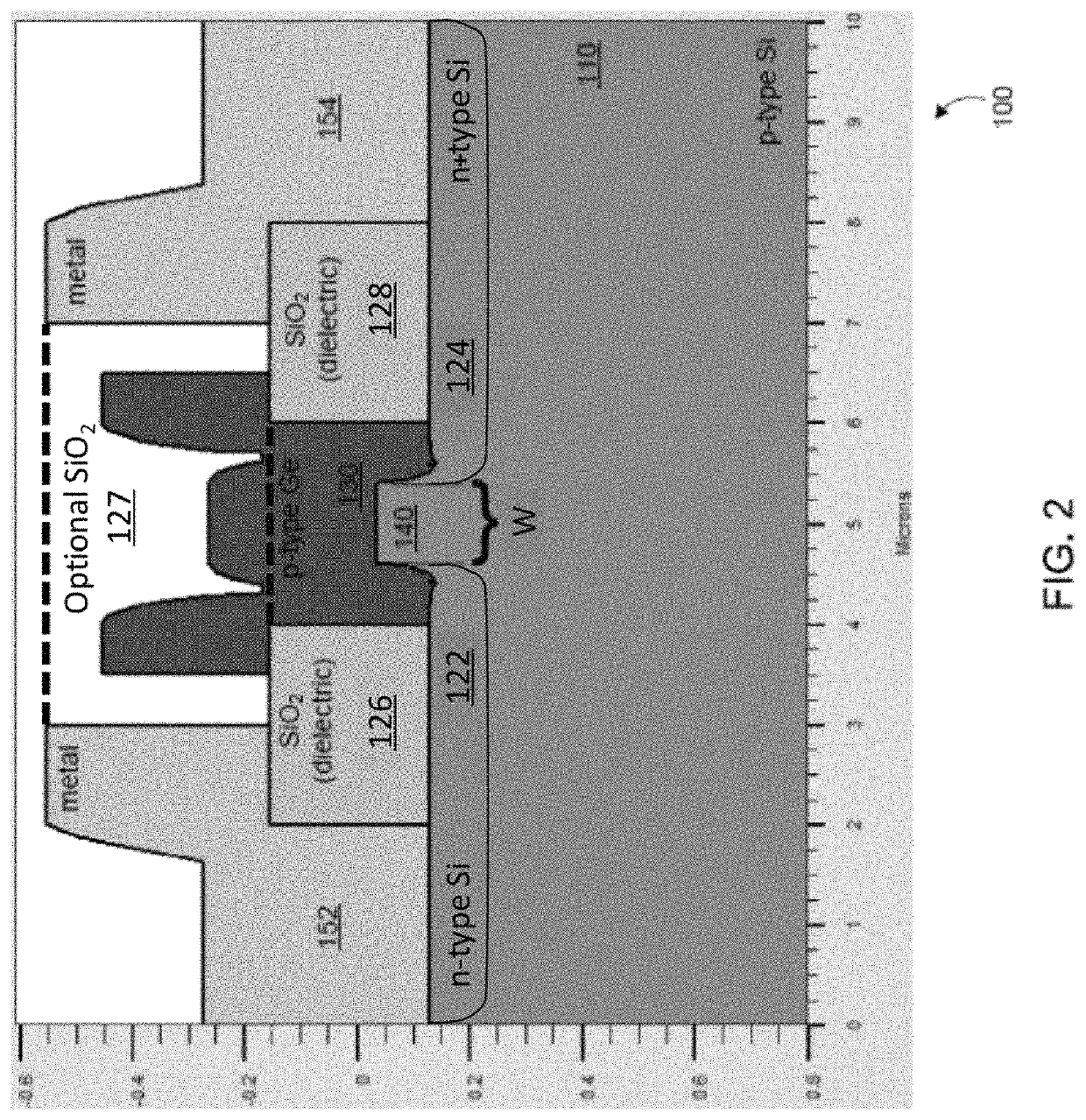
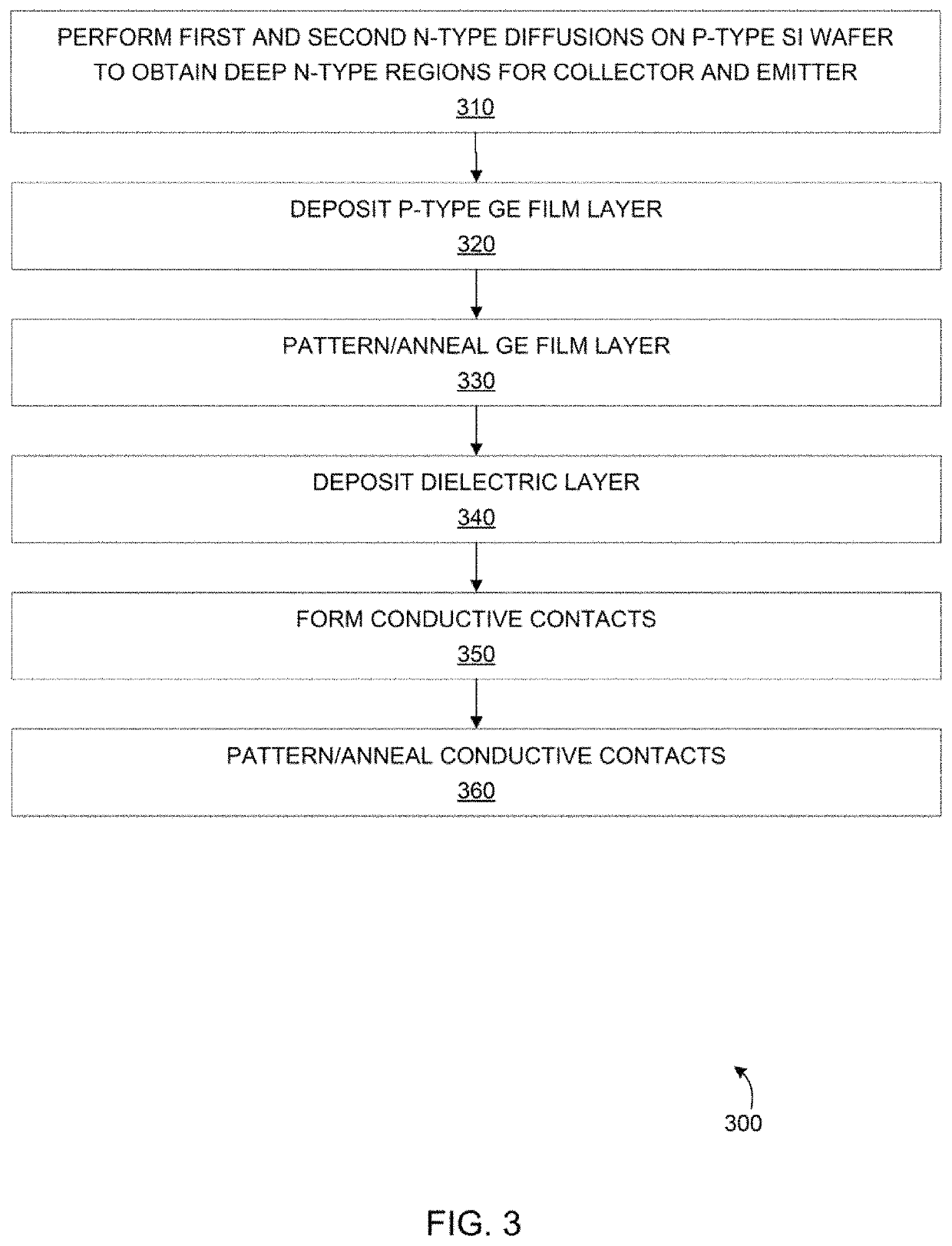
Si—Ge—Si phototransistor
a phototransistor and photodiode technology, applied in the field of detection light, can solve the problems of limited photodiodes, inability to fully meet the future requirements for speed, form/shape, responsivity, etc., and achieve the effect of enhancing the mobility of electric motors
- Summary
- Abstract
- Description
- Claims
- Application Information
AI Technical Summary
Benefits of technology
Problems solved by technology
Method used
Image

Examples
Embodiment Construction
[0016]The following description and drawings merely illustrate the principles of the invention. It will thus be appreciated that those skilled in the art will be able to devise various arrangements that, although not explicitly described or shown herein, embody the principles of the invention and are included within its scope. Furthermore, all examples recited herein are principally intended expressly to be only for illustrative purposes to aid the reader in understanding the principles of the invention and the concepts contributed by the inventor(s) to furthering the art, and are to be construed as being without limitation to such specifically recited examples and conditions. Additionally, the term, “or,” as used herein, refers to a non-exclusive or, unless otherwise indicated (e.g., “or else” or “or in the alternative”). Also, the various embodiments described herein are not necessarily mutually exclusive, as some embodiments can be combined with one or more other embodiments to f...
PUM
 Abstract
Description
Claims
Application Information