
Semiconductor device and manufacturing method thereof
a technology of semiconductor devices and semiconductor shields, applied in semiconductor devices, diodes, electrical devices, etc., can solve the problems of reducing the esd resistance together with the lowering of current capacity, increasing the required area of protection diodes, and difficulty in reducing the size of semiconductor devices, so as to reduce the size of trenches and electrical characteristics. , to achieve the effect of suppressing the degradation of the esd resistance of the gate protection diodes, reducing the size o
Patent Information
- Authority / Receiving Office
- US · United States
- Patent Type
- Patents(United States)
- Current Assignee / Owner
- Publication Date
- 2022-01-11
Smart Images
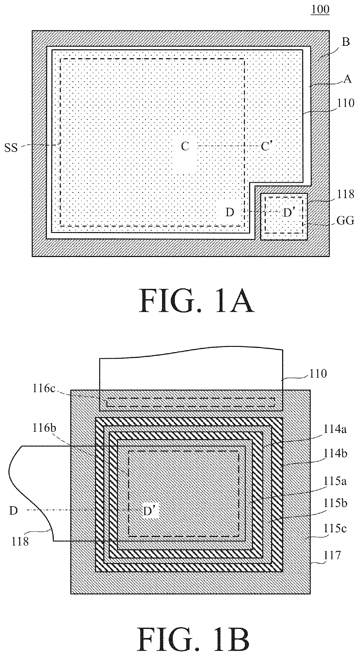
Figure 1 
Figure 2 
Figure 3
Abstract
Description
RELATED APPLICATIONS
[0001] This application claims priority to Japanese Patent Application No. 2019-065171, filed on Mar. 29, 2019, the entire content of which is incorporated herein by reference.BACKGROUND OF THE INVENTION1. Field of the Invention
[0002] The present invention relates to a semiconductor device, in particular to a semiconductor device having a gate protection diode and a vertical transistor which includes a trench gate and a gate insulating film.2. Description of the Related Art
[0003] A semiconductor device having a vertical transistor which includes a gate insulating film usually has a gate protection diode which protects the gate insulating film from an ESD (Electro-Static Discharge) or the like. Such a protection diode is formed of a polysilicon film or the like provided on the insulating film and made from the same polysilicon layer which constitutes a gate.
[0004] Japanese Patent Application Laid-open No. 2006-93505 discloses a technology in which a polysilicon layer ...
Examples
Embodiment Construction
[0025]An embodiment of the present invention will hereinafter be described with reference to the accompanying drawings. The drawings used in the following description may be shown with being partly omitted, enlarged and seen through in order to make the features of the present invention easier to understand, and their dimension ratios may be different from the actual ones. Incidentally, the same components are denoted by the same reference numerals, and their duplicated explanations will be omitted as appropriate.
[0026]FIG. 1A is a schematic plan view to describe a semiconductor device 100 having a vertical MOSFET with trench gate according to the embodiment of the present invention. FIG. 1B is a schematic plan view showing the vicinity of a gate pad GG in FIG. 1A which is enlarged and partly seen through.
[0027]As illustrated in FIG. 1A, the semiconductor device 100 includes an active region A and a field region B provided along the perimeter of the active region A. The vertical MOS...