Organic light emitting diode display device

a light-emitting diode and display device technology, applied in the direction of diodes, organic semiconductor devices, semiconductor devices, etc., can solve the problems of deteriorating emission properties, electrodes of organic display elements may be broken, and emission properties deteriorated

Active Publication Date: 2022-01-25
LG DISPLAY CO LTD
View PDF39 Cites 0 Cited by
  • Summary
  • Abstract
  • Description
  • Claims
  • Application Information

AI Technical Summary

Benefits of technology

[0010]One or more aspects of the present disclosure relate to an organic display element where permeation of an oxygen and a moisture and deterioration of an emission property are prevented by an organic layer including a self-healing material even when a barrier layer has a crack.

Problems solved by technology

An organic display element of an organic light emitting diode display device has a disadvantage that an emission property is deteriorated according to a time elapse.
An oxygen and a moisture may permeate the organic display element to deteriorate an organic layer and an electrode, thereby an emission property deteriorated.
However, when the barrier layer has a crack, an electrode of an organic display element may be broken due to permeation of an oxygen and a moisture.
Specifically, a crack and permeation of an oxygen and a moisture may remarkably occur in an organic display panel of plastic, i.e., a flexible organic display panel such as a bendable panel, a rollable panel and a foldable panel.

Method used


Image

  • Organic light emitting diode display device
  • Organic light emitting diode display device
  • Organic light emitting diode display device

Examples


first embodiment

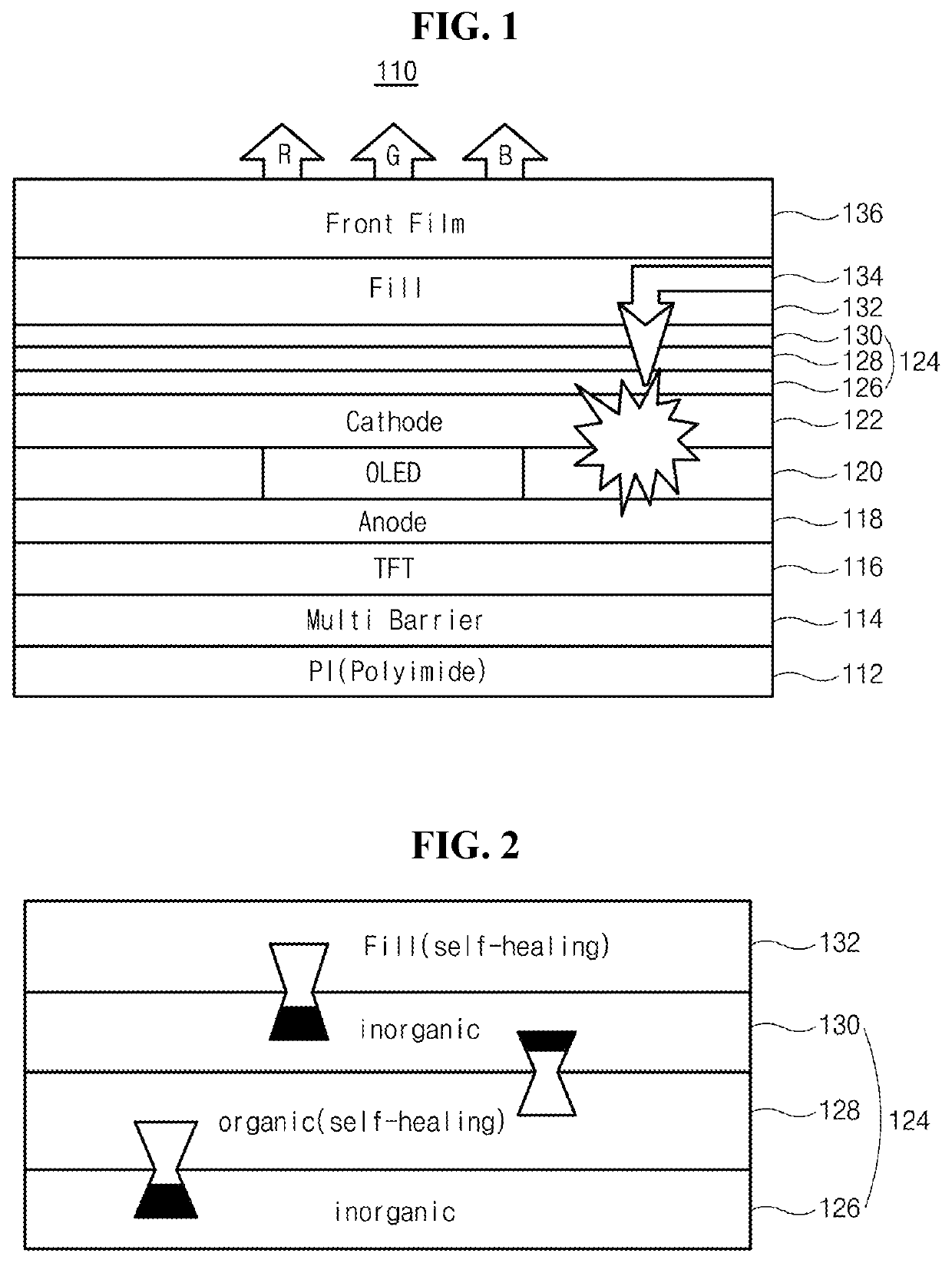
[0022]FIG. 1 is a cross-sectional view showing an organic display element according to the present disclosure.

[0023]In FIG. 1, an organic display element 110 includes a substrate 112, a multiple barrier 114, a thin film transistor (TFT) 116, a first electrode 118, an organic light emitting diode (OLED) 120, a second electrode 122, a barrier layer 124, a filler layer 132 and a front film 136. The substrate 112 may include a coloring polyimide (PI). The first and second electrodes 118 and 122 may be an anode and a cathode, respectively. The OLED 120 may include a single organic emitting layer. Alternatively, the OLED 120 may include at least two organic emitting layers such that the OLED 120 has a tandem structure.

[0024]The barrier layer 124 may include a first inorganic layer 126, an organic layer 128 and a second inorganic layer 130. The organic layer 128 may include one of acrylic resin and epoxy resin. The first and second inorganic layers 126 and 130 may include one of silicon ox...

second embodiment

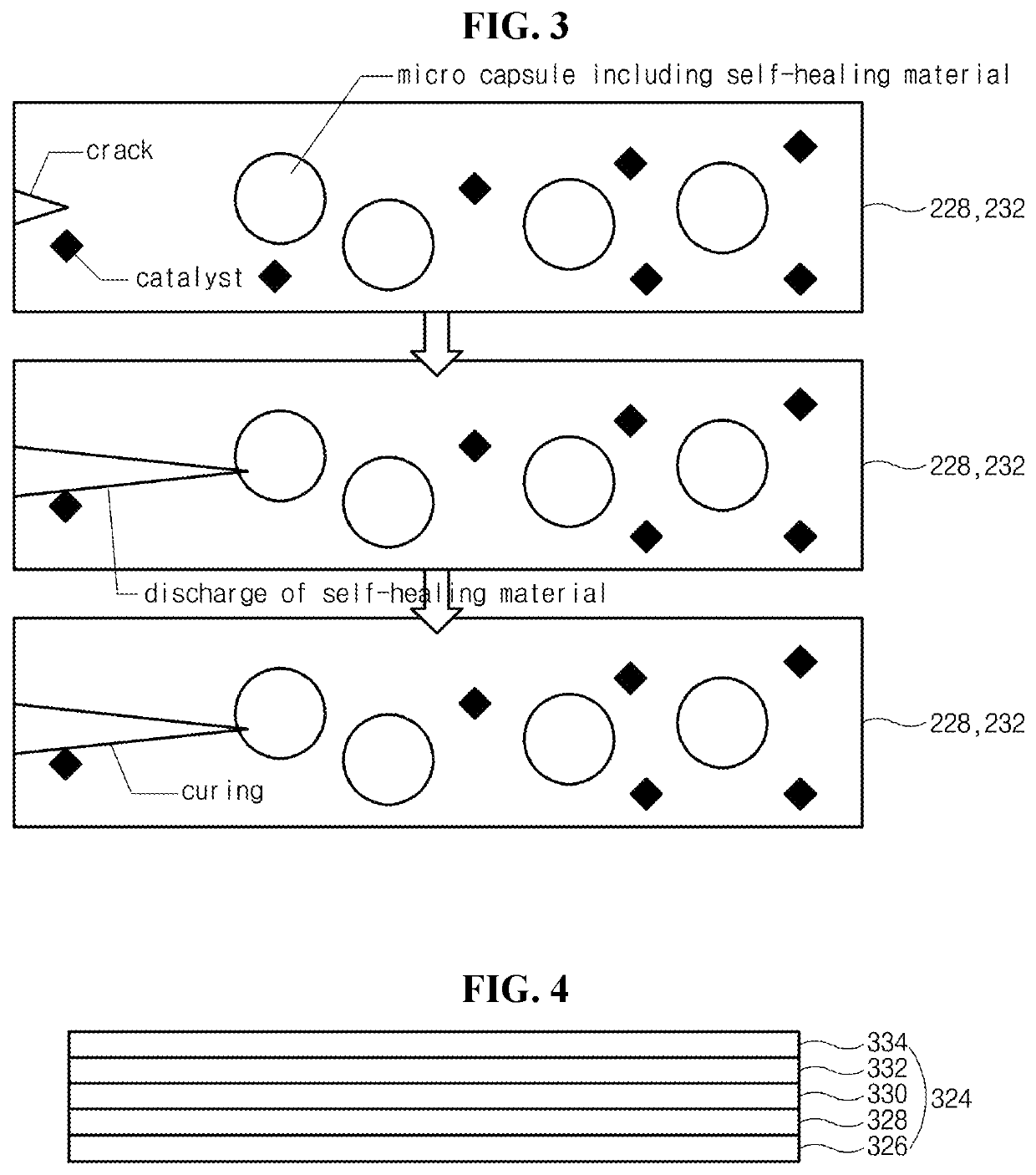
[0045]FIG. 3 is a cross-sectional view showing a mechanism of preventing extension of a crack due to a micro capsule of a barrier layer of an organic display element according to the present disclosure.

[0046]In FIG. 3, first and second organic layers 228 and 232 of a barrier layer of an organic display element include a micro capsule. For example, when the polymerizable monomer is used as the chemically self-healing material, the micro capsule may include both of the polymerizable monomer and the polymerization initiating catalyst. Alternatively, the micro capsule may include one of the polymerizable monomer and the polymerization initiating catalyst and the first and second organic layers 228 and 232 may include the other of the polymerizable monomer and the polymerization initiating catalyst.

[0047]The polymerizable monomer is discharged from the micro capsule due to an impact / a reaction of a crack generation, and the chemically self-healing material fills a whole or a part of the ...

fifth embodiment

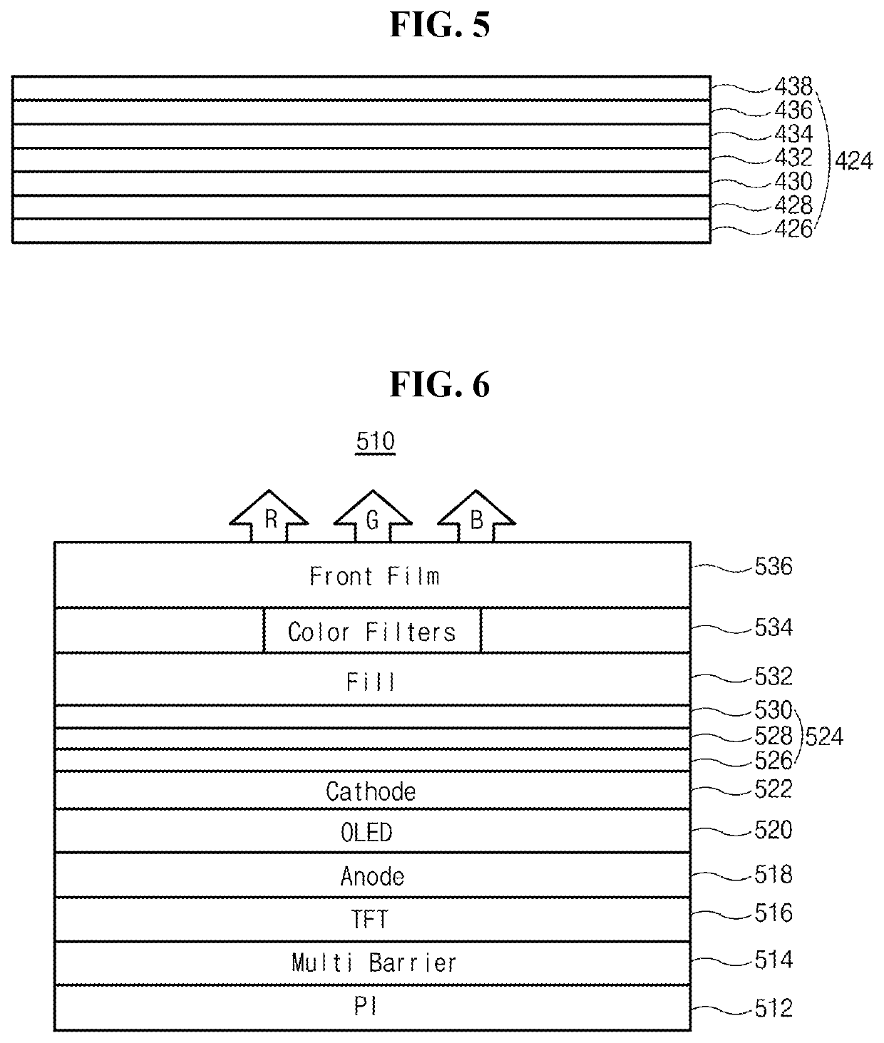
[0053]FIG. 6 is a cross-sectional view showing an organic display element according to the present disclosure.

[0054]The organic display element 110 has a division coloring type, and the OLED 120 of the organic display element 110 includes red, green and blue emitting layers in FIG. 1. In FIG. 6, an organic display element 510 includes a substrate 512, a multiple barrier 514, a thin film transistor (TFT) 516, a first electrode 518, an organic light emitting diode (OLED) 520, a second electrode 522, a barrier layer 524, a filler layer 532, a color filter layer 534 and a front film 536. The substrate 512 may include a coloring polyimide (PI). The first and second electrodes 518 and 522 may be an anode and a cathode, respectively.

[0055]The barrier layer 524 may include a first inorganic layer 526, an organic layer 528 and a second inorganic layer 530. The organic layer 528 may include one of acrylic resin and epoxy resin. The first and second inorganic layers 526 and 530 may include one...


PUM

PropertyMeasurementUnit
flexibleaaaaaaaaaa
phase separationaaaaaaaaaa
stressaaaaaaaaaa

Abstract

A display device includes: a substrate; a thin film transistor on the substrate; a first electrode, a light emitting diode and a second electrode sequentially on the thin film transistor; a barrier layer on the second electrode, the barrier layer including at least one organic layer; and a front film on the barrier layer, wherein the at least one organic layer includes a chemically self-healing material.

Description

CROSS-REFERENCE TO RELATED APPLICATION[0001]This application claims the benefit of Japanese Patent Application No. 2017-104185, filed on May 26, 2017, in the Japan Patent Office, which is incorporated herein by reference in its entirety.BACKGROUNDTechnical Field[0002]The present disclosure relates to a display device, touch display device, and more particularly, to an organic light emitting diode display device including a self-healing material.Description of the Background[0003]An organic display element of an organic light emitting diode display device has a disadvantage that an emission property is deteriorated according to a time elapse. An oxygen and a moisture may permeate the organic display element to deteriorate an organic layer and an electrode, thereby an emission property deteriorated. As a result, various means such as a sealant for blocking contact of the organic display element with an oxygen and a moisture are provided.[0004]For example, in a Japanese Patent Publicat...

Claims


Application Information

Patent Timeline
Patent Type & Authority Patents(United States)
IPC IPC(8): H01L51/52H01L51/00H01L27/32
CPCH01L51/529H01L51/0097H01L51/5256H01L51/5278H01L27/322H01L27/3244H01L2251/5338H01L2251/568H10K59/12H10K50/844H10K59/38H10K50/8445H10K50/87H10K71/861H10K77/111H10K50/18H10K50/11H10K50/84H10K50/19H10K2102/311
Inventor SATO, OSAMU
Owner LG DISPLAY CO LTD
Why Eureka
Try Eureka