Apparatus and method for manufacturing stress-free flexible printed circuit board

a printed circuit board and flexible technology, applied in the direction of electrolysis components, vacuum evaporation coatings, coatings, etc., can solve the problems of difficult stress control, inability to cope with high density wiring required in the semiconductor industrial, and vulnerability in terms of dimensional stability and flexibility of final products, so as to improve adhesiveness

Active Publication Date: 2013-01-15
RES & BUSINESS FOUND SUNGKYUNKWAN UNIV
View PDF14 Cites 1 Cited by
  • Summary
  • Abstract
  • Description
  • Claims
  • Application Information

AI Technical Summary

Benefits of technology

[0010]Accordingly, the present invention has been made to solve the above-mentioned problems occurring in the prior art and the present invention is to provide a method for manufacturing a flexible circuit board, which is adapted to fabricate a highly efficient flexible thin metal (e.g., copper) film-laminated strip by improving adhesiveness between a substrate (e.g., polyimide strip) and a metal thin film through magnetron sputtering, which is a dry deposition process, and by removing stress from laminated metal films formed through magnetron sputtering.
[0015]The inventive method may further include a step of forming a moisture and oxygen barrier film on the surface of the polyimide strip opposite to the thick metal film from an oxide and a nitride after the thick copper film is formed in step (c) so as to prevent permeation of moisture and oxygen.

Problems solved by technology

With these methods, it is impossible to cope with high density wiring required in the semiconductor industrial due to difficulty in finely processing such a metal film in a width of not more than 10 μm because the thermal performance of the adhesive is inferior to that of the substrate (e.g., polymer strip), and the resultant metal film formed by the methods has a thickness of not less than 10 μm, which is too thick to be finely processed.
In addition, the above-mentioned methods reveal vulnerability in terms of dimensional stability and flexibility of a final product.
Like this, when forming a laminated film with a thickness of several or more microns, wet electroplating is also carried out in combination with a dry deposition process because it is difficult to control stress only with a dry deposition process.
If wet electroplating is also employed, a process for manufacturing a flexible metal (e.g., copper) film-laminated strip is complicated, and a manufacturing space should be increased.
As a result, manufacturing costs and time are substantially increased.
Furthermore, the electroplating has a problem of causing environmental pollution.
However, if thin metal (e.g., copper) films to be laminated are formed completely through a dry deposition process, a metal film-laminated strip is liable to be deformed due to the stress induced in the laminated film as the thickness of the metal film is increased.
Thus, it cannot be assured to obtain a thickness of several or more microns for the copper film-laminated strip.

Method used


Image

  • Apparatus and method for manufacturing stress-free flexible printed circuit board
  • Apparatus and method for manufacturing stress-free flexible printed circuit board
  • Apparatus and method for manufacturing stress-free flexible printed circuit board

Examples


Embodiment Construction

[0024]Hereinafter, a preferred embodiment of the present invention will be described with reference to the accompanying drawings. In the following description and drawings, the same reference numerals are used to designate the same or similar components.

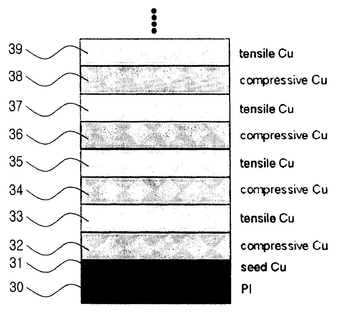
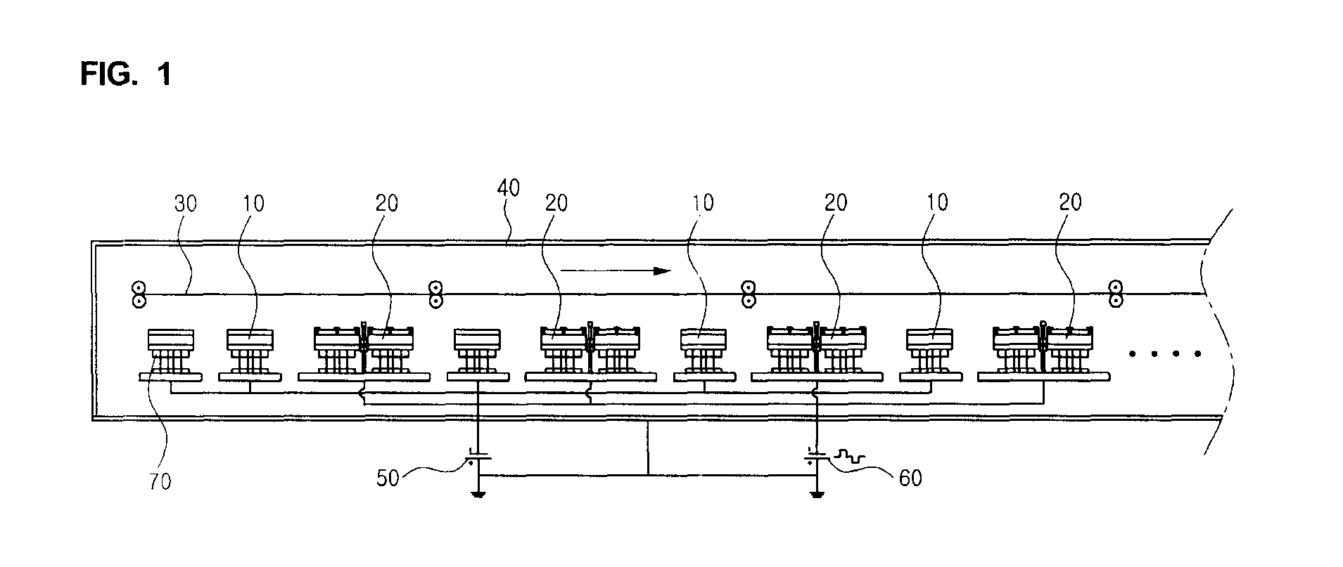
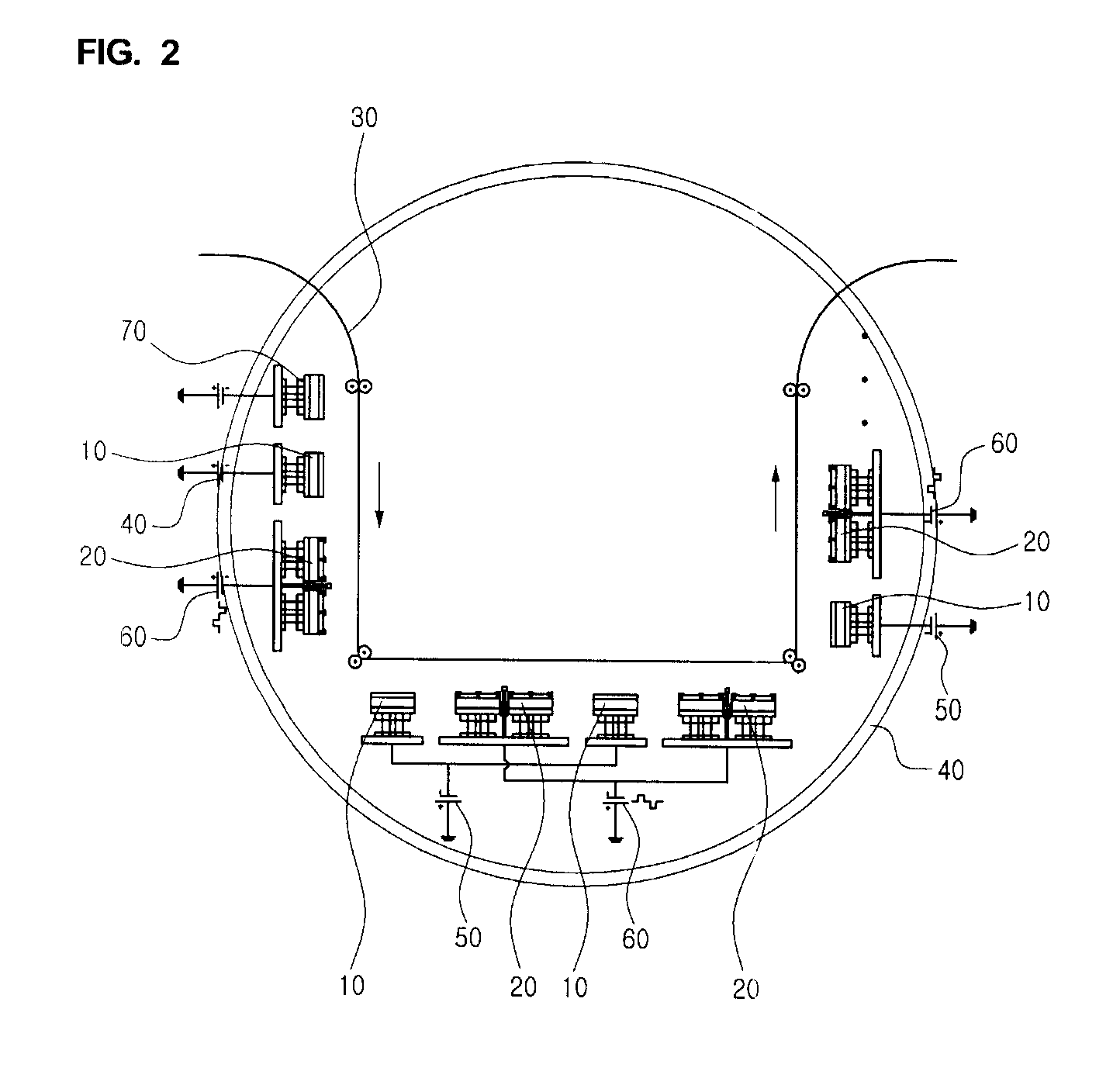
[0025]FIG. 1 shows an example of a magnetron sputtering apparatus, to which a method of manufacturing a flexible circuit board according to the present invention is applied, and FIG. 4 shows a cross-section of a stress-free flexible copper film-laminated strip deposited according to a method of manufacturing a flexible circuit board according to the present invention. The magnetron sputtering apparatus includes a plurality of single magnetron deposition sources 10, a plurality of dual magnetron deposition sources 20, and a substrate 30, the magnetron deposition sources 10 and 20, and the substrate 30 being installed within a vacuum chamber 40. Each of the single magnetron deposition sources 10 and the dual magnetron deposition source...


PUM

PropertyMeasurementUnit
thicknessaaaaaaaaaa
widthaaaaaaaaaa
wavelengthaaaaaaaaaa

Abstract

An apparatus and method for manufacturing a highly efficient flexible thin metal film-laminated strip by improves adhesiveness between a polyimide strip and a thin metal film, and removes stress from thin films laminated through magnetron sputtering, which is a dry deposition process. The stress-free flexible circuit board manufacturing method includes the steps of: a) depositing a seed layer on the substrate using the magnetron deposition source; b) depositing a compressive thin film using the single magnetron deposition source arranged next to the magnetron deposition source; c) depositing tensile thin film using the dual magnetron deposition source arranged next to the single magnetron deposition source; and d) repeating the steps b) and c) so as to sequentially and alternately deposit compressive thin films and tensile thin films thereby obtaining a thick film with a desired thickness.

Description

CROSS REFERENCES TO RELATED APPLICATIONS[0001]This application claims the priority benefit of Korean patent application No. 10-2007-0017716 filed on Feb. 22, 2007, and is fully incorporated herein by reference.STATEMENT REGARDING FEDERALLY SPONSORED RESEARCH[0002]Not Applicable.FIELD OF INVENTION[0003]The present invention relates to an apparatus and method for manufacturing a flexible printed circuit board, and more particularly to an apparatus and method for manufacturing a highly efficient flexible thin metal film-laminated strip by improving adhesiveness between a substrate (e.g., polyimide strip) and a thin metal film, and removing stress from thin metal films formed through magnetron sputtering, which is a dry deposition process.BACKGROUND OF INVENTION[0004]Such a thin metal film-laminated strip may be fabricated by heating and pressing a rolled or electrolytic metal film (e.g., copper film), or the like on an adhesive-coated surface of a plastic strip (e.g., polyimide strip),...

Claims


Application Information

Patent Timeline
Patent Type & Authority Patents(United States)
IPC IPC(8): C23C14/00
CPCC23C14/20C23C14/352C23C14/562H01J37/3277H01J37/3405H05K1/028H05K1/09H05K3/16H05K2201/0317H05K2201/0338H05K2203/1476H05K2203/1545H05K3/00
Inventor HAN, JEON GEONKIM, KAB SEOGKIM, YONG MO
Owner RES & BUSINESS FOUND SUNGKYUNKWAN UNIV
Why Eureka
Try Eureka