

Photosensitive field-effect transistor
a field-effect transistor and photosensitive technology, applied in the direction of photovoltaic energy generation, electrical apparatus, semiconductor devices, etc., can solve the problems of inability to use similar electrical shutters in photodetectors, inability to perform and inability to achieve complete resets of shutters. , to achieve the effect of facilitating the use of cds method, high frame rate and charge neutrality of photoactive materials
- Summary
- Abstract
- Description
- Claims
- Application Information
AI Technical Summary
Benefits of technology
Problems solved by technology
Method used
Image

Examples
Embodiment Construction
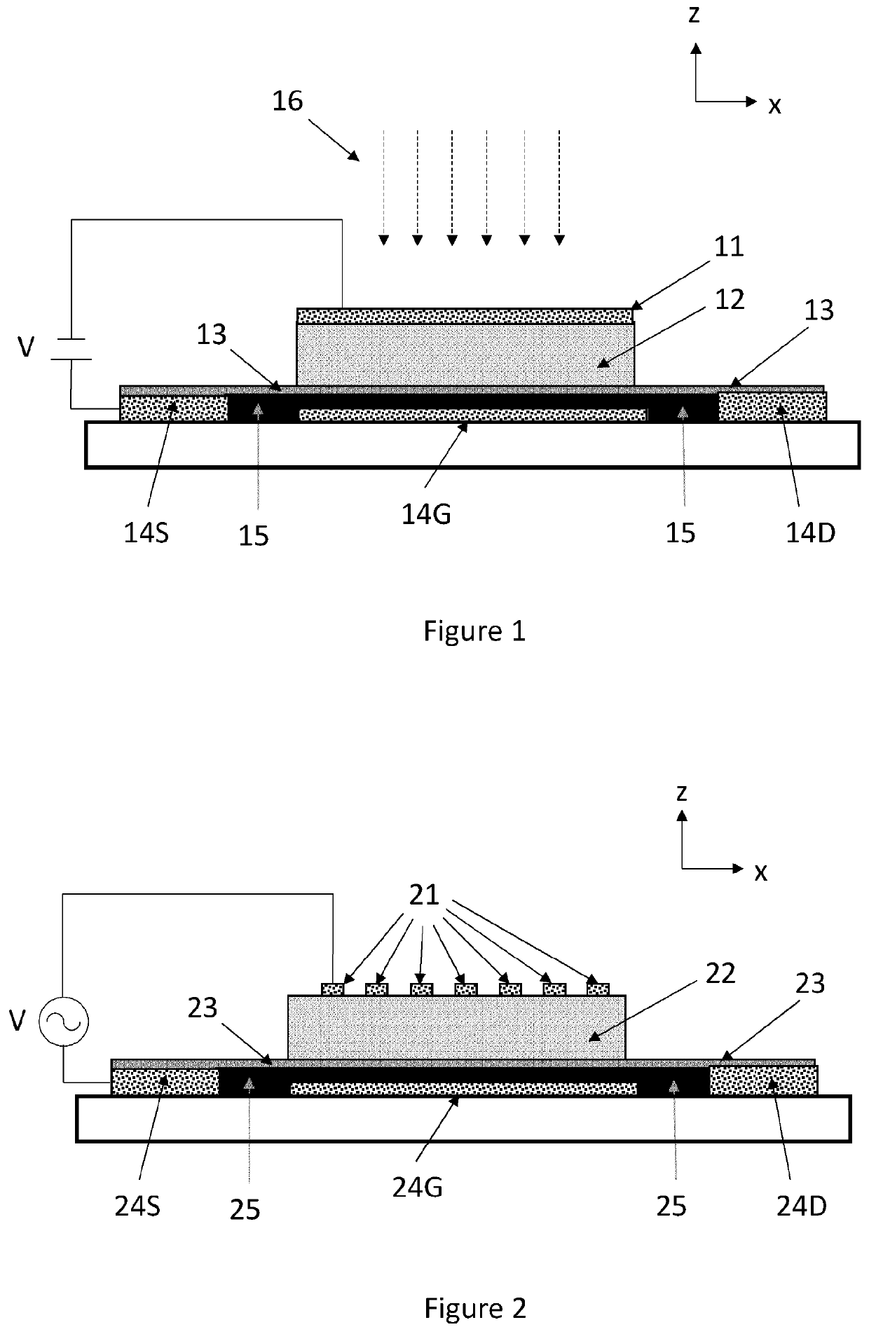
[0026]It is known that the flow of charge carriers from a photoactive layer to a channel of two-dimensional material in an illuminated photosensitive field-effect transistor can be altered with an external bias. The flow current depends on the magnitude and the direction of the bias voltage. FIG. 1 illustrates schematically a photosensitive field-effect transistor which comprises source (14S), drain (14D) and gate (14G) electrodes on the surface of a substrate, a channel (13) deposited on the surface and an insulating layer (15) between the first gate electrode (14G) and the channel (13). The transistor also comprises a photoactive layer (12) which partly covers the channel (13), and a second gate electrode (11) which covers the photoactive layer (12). Electromagnetic radiation (16) illuminates the photosensitive transistor.
[0027]A bias voltage V applied between the second gate electrode 11 and the channel 13 can alter the electrical characteristics of the interface between the phot...
PUM
| Property | Measurement | Unit |
|---|---|---|
| diameter | aaaaa | aaaaa |
| thickness | aaaaa | aaaaa |
| thickness | aaaaa | aaaaa |
Abstract
Description
Claims
Application Information