Feedback 1T DRAM device having localized partial insulating layers

a dram device and partial insulating technology, applied in the direction of semiconductor devices, electrical devices, transistors, etc., can solve the problems of limiting the current slope (i.e., subthreshold swing) in a subthreshold voltage due, limiting the retention time, and always applying hold voltage, so as to reduce the loss of carriers, improve operation reliability, and maximize retention time

Active Publication Date: 2022-04-05
GACHON UNIV OF IND ACADEMIC COOPERATION FOUND
View PDF6 Cites 0 Cited by
  • Summary
  • Abstract
  • Description
  • Claims
  • Application Information

AI Technical Summary

Benefits of technology

[0007]The present invention provides a feedback 1T DRAM having a partial insulating layer to maximize retention time and improve operation reliability by reducing carriers lost beyond the energy barrier due to p-n junction even in a p-n-p-n structure by impurity doping.
[0020]In the present invention, a body region may be divided into two or more in a channel direction by pn junctions and / or partial insulating layers, and gates may be formed on each of the divided body regions. The present invention can be operated by filling and subtracting electrons in the energy well of the conduction band and holes in the energy well of the valence band, respectively. In addition, it is possible to maximize retention time and improve operation reliability by reducing carrier loss by energy barriers of pn junctions and / or partial insulating layers.

Problems solved by technology

However, in the case of MOSFET transistors, when the current flows between the source and the drain by the gate voltage, there is a limit to the current slope (i.e., Subthreshold Swing) in a subthreshold voltage due to the heat dissipation mechanism.
Therefore, there is a problem in that a hold voltage should always be applied.
There is a problem that a hold voltage should always be applied. germanium shell.

Method used


Image

  • Feedback 1T DRAM device having localized partial insulating layers
  • Feedback 1T DRAM device having localized partial insulating layers
  • Feedback 1T DRAM device having localized partial insulating layers

Examples


Embodiment Construction

[0030]Detailed descriptions of preferred embodiments of the present invention are provided below with accompanying drawings.

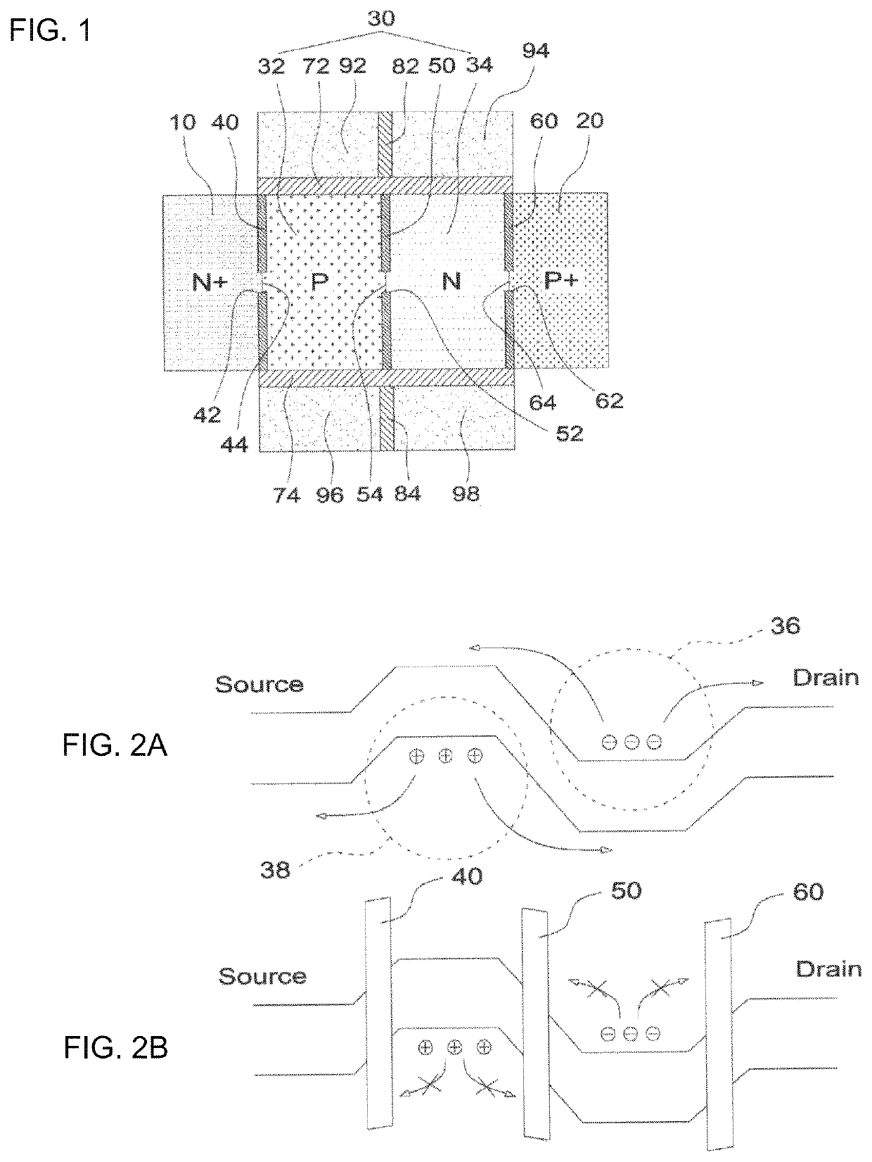
[0031]A 1T DRAM device according to an embodiment of the present invention, as shown in FIG. 1, comprises source region 10 and drain region 20; a body region 30 having two or more doped semiconductor layers 32 and 34 connected by a pn junction 54 in a channel direction between the source and drain regions 10 and 20; and a plurality of gates 92, 94, 96, and 98 formed on each of the doped semiconductor layers with a gate insulating layer 72 or 74 interposed therebetween.

[0032]In the above embodiment, a source partial insulating layer 40, a body partial insulating layer 50, and a drain partial insulating layer 60 which will be described later with reference to FIG. 1 are absent. In FIG. 1, the source region 10 is an N+ doped layer as a first conductivity type semiconductor layer, and the body region 30 consist of a P doped layer 32 which is a second conductivity t...


PUM


Abstract

A feedback 1T DRAM device that has a partial insulating film structure is provided. A body region may be divided into two or more in a channel direction by pn junctions and / or partial insulating layers, and gates may be formed on each of the divided body regions. The present invention can be operated by filling and subtracting electrons in the energy well of the conduction band and holes in the energy well of the valence band, respectively. In addition, it is possible to maximize retention time and improve operation reliability by reducing carrier loss by energy barriers of pn junctions and / or partial insulating layers.

Description

CROSS-REFERENCE TO RELATED APPLICATION[0001]This application claims priority to Korean Patent Application No. 10-2019-0105435, filed on Aug. 27, 2019, under 35 U.S.C. 119, the entire contents of which are hereby incorporated by reference. by reference.BACKGROUNDField of the Invention[0002]The present invention relates to a dynamic random access memory (DRAM) device, and more particularly to a feedback 1T DRAM device having a partial insulating film structure.Related Art[0003]DRAM is a typical volatile memory, which has advantages of high operating speed and high integration and serves as a main memory device in computers and electronic systems. The electrons or holes are stored to have a memory characteristic, and as time passes, the electrons or holes are dissipated, and thus a periodic refresh operation is required. In general, DRAM has a structure consisting of one transistor and one capacitor (1T1C structure) but may have a 1T DRAM structure in which capacitors are removed to fu...

Claims


Application Information

Patent Timeline
Patent Type & Authority Patents(United States)
IPC IPC(8): H01L27/108H01L29/78
CPCH01L27/10802H01L27/10805H01L27/10847H01L29/7841H01L29/7455H01L27/1027H01L29/0653H10B12/10H10B12/00H01L29/0615H01L29/41725H01L29/0646H01L29/42312H01L27/098H10B12/01H10B12/30H10B12/20H10B12/02
Inventor CHO, SEONGJAE
Owner GACHON UNIV OF IND ACADEMIC COOPERATION FOUND
Why Eureka
Try Eureka