Dielectric structure applied to building components for increasing transmittance of RF signal and disposing method thereof
- Summary
- Abstract
- Description
- Claims
- Application Information
AI Technical Summary
Benefits of technology
Problems solved by technology
Method used
Image
Examples
Embodiment Construction
[0022]To facilitate the review of the technical features, contents, advantages, and achievable effects of the present invention, the embodiments together with the accompanying drawings are described in detail as follows. However, the drawings are used only for the purpose of indicating and supporting the specification, which is not necessarily the real proportion and precise configuration after the implementation of the present invention. Therefore, the relations of the proportion and configuration of the accompanying drawings should not be interpreted to limit the actual scope of implementation of the present invention.
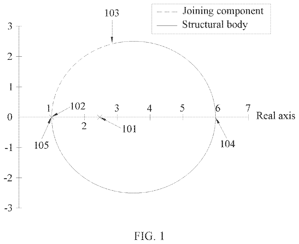
[0023]Please refer to FIG. 1, which illustrates an admittance chart according to the prior art. Take a joining component (shown by position 101) of εs=εr=6 being placed in an environment (shown by position 102) of εr=1 as an example. As the thickness of the joining component gradually increases from 0 to ts, the admittance value αs moves from position 102 to position...
PUM
 Abstract
Description
Claims
Application Information


