Method for correcting mask pattern and mask pattern thereof

a mask pattern and mask pattern technology, applied in the direction of microlithography exposure apparatus, photomechanical treatment, instruments, etc., can solve the problems of physical limitations, distortion of the mask pattern, and physical limitation of the distance between the above components, so as to avoid the occurrence of necking or breaking

Active Publication Date: 2022-06-28
UNITED MICROELECTRONICS CORP
View PDF17 Cites 0 Cited by
  • Summary
  • Abstract
  • Description
  • Claims
  • Application Information

AI Technical Summary

Benefits of technology

[0005]The present invention provides a method for correcting a mask pattern, and a mask pattern thereof, to avoid the occurrence of necking or breaking on portion of the post-transfer pattern.
[0017]In the method for correcting a mask pattern according to the embodiments of the present invention, the first pattern extends from the isolated pattern area to the dense pattern area and / or from the dense pattern area to the isolated pattern area, and by forming a slot on a transition zone of the first pattern, wherein the transition zone is a specific section of the first pattern located on the transition area of the isolated pattern region and the dense pattern region, the light energy on the transition zone of the first pattern is dispersed during the exposure and development process of the mask pattern, so that the light energy is not excessively concentrated on the transition zone of the first pattern, to avoid the occurrence of necking or breaking on portion of the post-transfer pattern.

Problems solved by technology

However, the distance between the above components may be physically limited in the exposure process due to the influence of optical characteristics.
Moreover, when the density of the light-transmitting areas on a mask is different, the light passing through the dense light-transmissive area will be affected by the light passing through the isolated light-transmissive area, to cause the exposed pattern to be distorted.

Method used


Image

  • Method for correcting mask pattern and mask pattern thereof
  • Method for correcting mask pattern and mask pattern thereof
  • Method for correcting mask pattern and mask pattern thereof

Examples


Embodiment Construction

[0023]The present invention will now be described more specifically with reference to the following embodiments. It is to be noted that the following descriptions of preferred embodiments of this invention are presented herein for purpose of illustration and description only. It is not intended to be exhaustive or to be limited to the precise form disclosed.

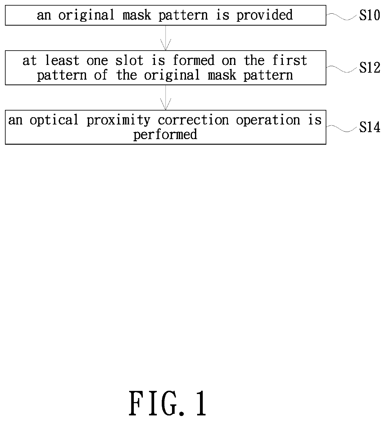
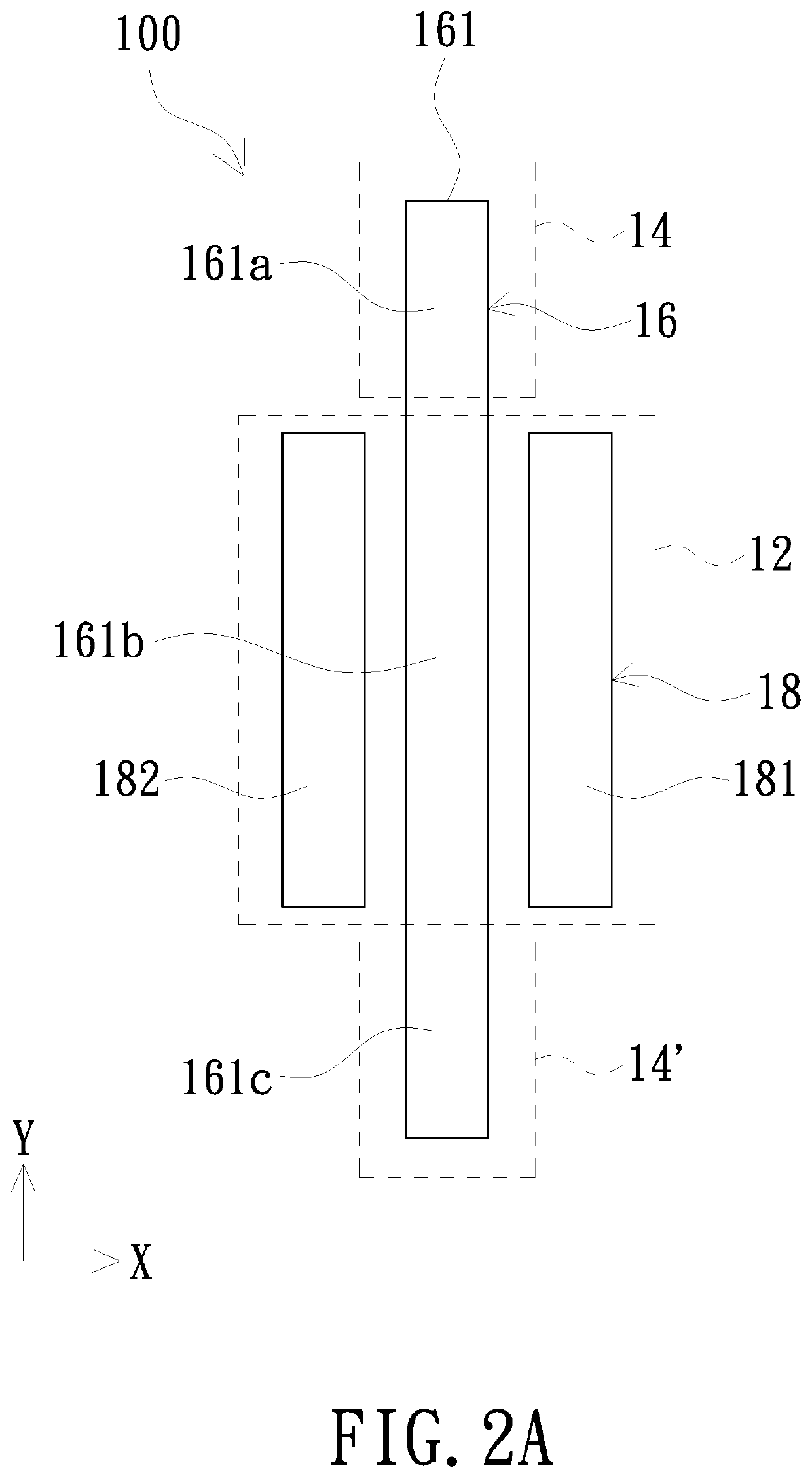
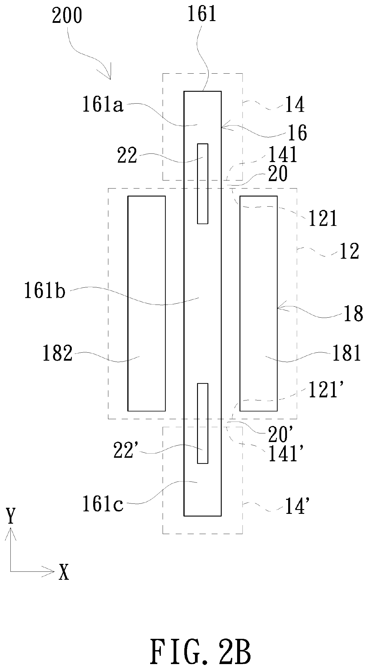
[0024]FIG. 1 is a schematic flow chart of a method for correcting a mask pattern according to one embodiment of the present invention, and FIG. 2A to FIG. 2C are schematic diagrams of various stages / steps of a method for correcting a mask pattern according to one embodiment of the present invention, wherein FIG. 2A illustrates an original mask pattern 100 at the beginning of the process, FIG. 2B illustrates a temporary mask pattern 200 having slots on the original mask pattern 100, and FIG. 2C illustrates a corrected mask pattern 300 after an optical proximity correction procedure (OPC) is performed.

[0025]Referring to FIG. 1 and ...


PUM

PropertyMeasurementUnit
optical proximity correctionaaaaaaaaaa
areaaaaaaaaaaa
distanceaaaaaaaaaa

Abstract

A method for correcting a mask pattern includes: providing an original mask pattern including at least one dense pattern area and at least one isolated pattern area, and the original mask pattern being divided into a first pattern and a second pattern, wherein the first pattern is formed in the isolated pattern area and extends to the dense pattern area, and the second pattern is formed in the dense pattern area; forming at least one slot on at least one section of the first pattern, and the at least one section of the first pattern is located on at least one transition area between the at least one isolated pattern area and the at least one dense pattern area; and performing an optical proximity correction operation on the first pattern formed with at least one slot and the second pattern. Using the corrected mask pattern may avoid the occurrence of necking or breaking on portion of the post-transfer pattern.

Description

FIELD OF THE INVENTION[0001]The present invention relates to a method for correcting a mask pattern, and more particularly to the method for correcting the mask pattern with isolated pattern area and dense pattern area, and the mask pattern thereof.BACKGROUND OF THE INVENTION[0002]Lithography involves the transfer of an image of a mask to a material layer of a die or chip, also referred to as a wafer. The image is formed in a layer of photoresist, the photoresist is developed, and the photoresist is used as a mask during a process to alter the material layer, such as etching and patterning the material layer.[0003]With the rapid development in the integrated level of semiconductor integrated circuits, the width of the line required by lithography is becoming smaller and smaller, and the distance between semiconductor components is also becoming shorter. However, the distance between the above components may be physically limited in the exposure process due to the influence of optica...

Claims


Application Information

Patent Timeline
Patent Type & Authority Patents(United States)
IPC IPC(8): G03F1/36G03F1/38G03F1/84G03F7/20
CPCG03F1/36G03F1/38G03F1/84G03F7/70441
Inventor SUN, CHIA-CHENTUNG, YU-CHENGHSUEH, SHENG-YUANLIN, FAN WEI
Owner UNITED MICROELECTRONICS CORP
Why Eureka
Try Eureka