Light irradiation type heat treatment method and heat treatment apparatus

a heat treatment method and heat treatment technology, applied in the direction of optical radiation measurement, measurement devices, instruments, etc., can solve the problems of a large amount of recovery work, a lot of time, and a broken semiconductor wafer

Active Publication Date: 2022-09-27
DAINIPPON SCREEN MTG CO LTD
View PDF33 Cites 0 Cited by
  • Summary
  • Abstract
  • Description
  • Claims
  • Application Information

AI Technical Summary

Benefits of technology

The patent aims to prevent breakage of a substrate and reduce treatment efficiency. Its technical effect is to prevent breakage of the substrate and maintain treatment efficiency.

Problems solved by technology

The bowing of the semiconductor wafer is caused by a heat treatment pattern of the halogen lamp or a problem that the semiconductor wafer itself has.
In either case, when the semiconductor wafer in the bowing state is irradiated with a flash of intense light for an extremely short time from the flash lamp, the semiconductor wafer may get broken.
When the wafer breakage occurs, the semiconductor wafer is wastefully consumed, and moreover, an inner portion of a chamber is contaminated by a large amount of particles, so that it takes a lot of time to perform a recovery work.

Method used


Image

  • Light irradiation type heat treatment method and heat treatment apparatus
  • Light irradiation type heat treatment method and heat treatment apparatus
  • Light irradiation type heat treatment method and heat treatment apparatus

Examples


Embodiment Construction

[0035]A preferred embodiment according to the present invention will now be described in detail with reference to the drawings.

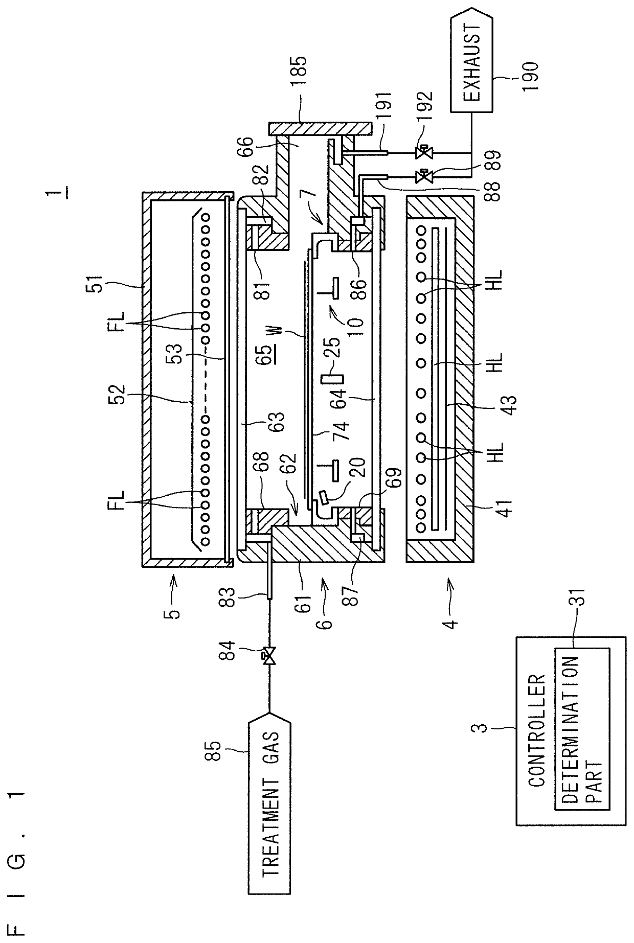
[0036]FIG. 1 is a longitudinal sectional view showing a configuration of a heat treatment apparatus 1 according to the present invention. The heat treatment apparatus 1 in FIG. 1 is a flash lamp annealer for heating a disk-shaped semiconductor wafer W serving as a substrate by irradiating the semiconductor wafer W with a flash of light. A size of the semiconductor wafer W to be treated is not particularly limited. For example, the semiconductor wafer W to be treated has a diameter of 300 mm or 450 mm (300 mm in the present preferred embodiment). An impurity is implanted into the semiconductor wafer W before being transported into the heat treatment apparatus 1, and a process of activating the implanted impurity is executed by a heat treatment in the heat treatment apparatus 1. It should be noted that dimensions of components and the number of components are ...


PUM


Abstract

After a semiconductor wafer held by a susceptor in a chamber is preheated by irradiating the semiconductor wafer with light from halogen lamps, the semiconductor wafer is irradiated with a flash of light from flash lamps. A temperature of the semiconductor wafer is measured with an end edge part radiation thermometer and a temperature of the susceptor is measured with a central part radiation thermometer. It is determined that the semiconductor wafer bows when a specific singular point appears in a temporal differentiation in the temperature measured with the end edge part radiation thermometer or a temporal differentiation in the temperature measured with the central part radiation thermometer. A flash light irradiation of the semiconductor wafer which is determined to be in the bowing state is omitted and the semiconductor wafer is transported out of the chamber, and the subsequent semiconductor wafer is transported into the chamber.

Description

BACKGROUND OF THE INVENTIONField of the Invention[0001]The present invention relates to a heat treatment method and heat treatment apparatus which irradiates a thin plate-like precision electronic substrate (hereinafter referred to simply as a “substrate”) such as a semiconductor wafer with light to heat the substrate.Description of the Background Art[0002]A flash lamp anneal (FLA) which heats a semiconductor wafer for an extremely short time in a process of manufacturing a semiconductor device attracts attention. The flash lamp anneal is a heat treatment technique of irradiating a surface of a semiconductor wafer with a flash of light using a xenon flash lamp (a simple term of “a flash lamp” means a xenon flash lamp hereinafter), thereby increasing a temperature of only the surface of the semiconductor wafer in an extremely short time (several milliseconds or less).[0003]A radiation spectral distribution of the xenon flash lamp ranges from an ultraviolet region to a near-infrared r...

Claims


Application Information

Patent Timeline
IPC IPC(8): H01L21/67
CPCH01L21/67115H01L21/67248H01L21/68707H01L21/6875H01L21/67288G01J5/0007
Inventor SHIGEMASU, SHOGOYAMADA, TAKAHIRO
Owner DAINIPPON SCREEN MTG CO LTD
Why Eureka
Try Eureka