

Apparatus and method for non-destructive, low stress removal of soldered electronic components
a technology of electronic components and apparatus, applied in the direction of ovens, lighting and heating apparatus, ovens, etc., can solve the problems of solder ball, uncompetitive chip manufacturer situations, and corresponding increases in overall chip failure rates
Inactive Publication Date: 2001-04-12
IBM CORP
View PDF0 Cites 5 Cited by
- Summary
- Abstract
- Description
- Claims
- Application Information
AI Technical Summary
Benefits of technology
44. It is an advantage of the invention that there is provided an improved method and apparatus for separating chips from chip carriers.45. It is an advantage of the invention that there is provided an improved method and apparatus for processing KGD chips, to remove them from the chip carrier while the solder connections are solid, such that substantially all of the solder remains attached to the chip.46. It is an advantage of the invention that there is provided an apparatus for removing chips from substrates where the force required is substantially the same for all chips or rows of chips.47. It is an advantage of the invention that there is provided a cascade effect apparatus and method for sequentially removing chips or rows of chips from one or more chip carriers, or substrates.48. It is an advantage of the invention that there is provided an apparatus comprising a single fixture for removing chips from a chip carrier and reforming solder on the chips for subsequent attachment.
Problems solved by technology
4. As technology has evolved, semiconductor devices have become smaller and more dense, which has resulted in corresponding increases in overall chip failure rates, which in turn results in uncompetitive situations for chip manufacturers.
These forces typically fracture the solder balls, leaving some solder attached to the substrate and some to the chip.
First, since components (carrier, chip, cavity, etc.) have inherent dimensional variability, an undetermined quantity of assemblies are subjected to the shear force in each run.
Consequently, the force per assembly is unknown and will most probably be insufficient to disassemble the solder in the solidus state from the substrate.
Second, a matrix of cavity rows and columns increases the apparatus' size and weight (vs the single cavity).
In one case, some assemblies could be under load but have insufficient temperature for disassembly in the solidus state.
In another case, some assemblies could be at the appropriate temperature range but not be under load, or sufficient load.
Method used
View moreImage
Smart ImageViewing Examples

Examples
Embodiment Construction
49. It will be appreciated that, although specific embodiments of the invention have been described herein for purposes of illustration, various modifications may be made without departing from the spirit and scope of the invention.
50. Accordingly, the scope of protection of this invention is limited only by the following claims and their equivalents.
Login to View More PUM
| Property | Measurement | Unit |
|---|---|---|
| Temperature | aaaaa | aaaaa |
| Force | aaaaa | aaaaa |
| Size | aaaaa | aaaaa |
Abstract
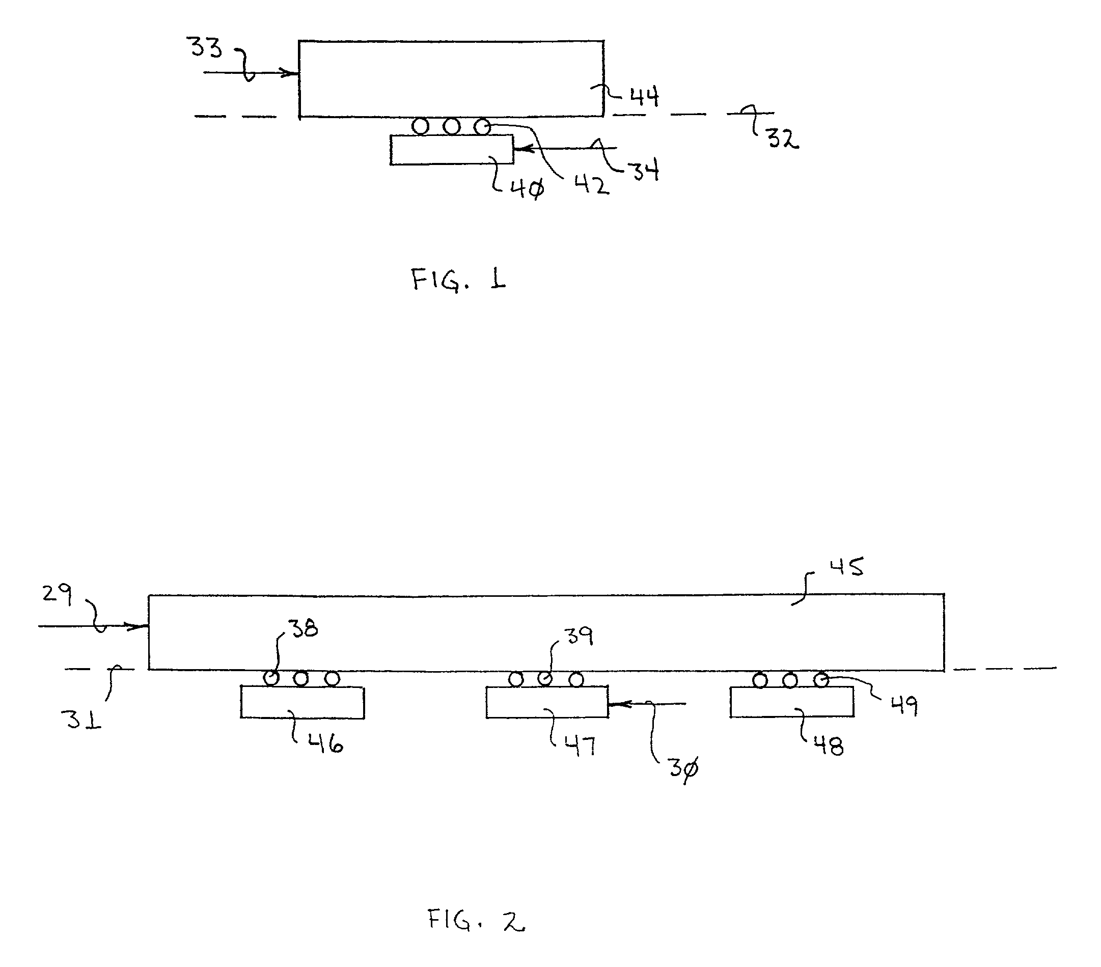
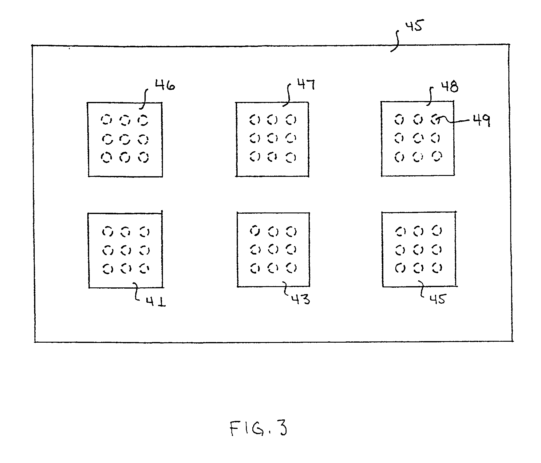
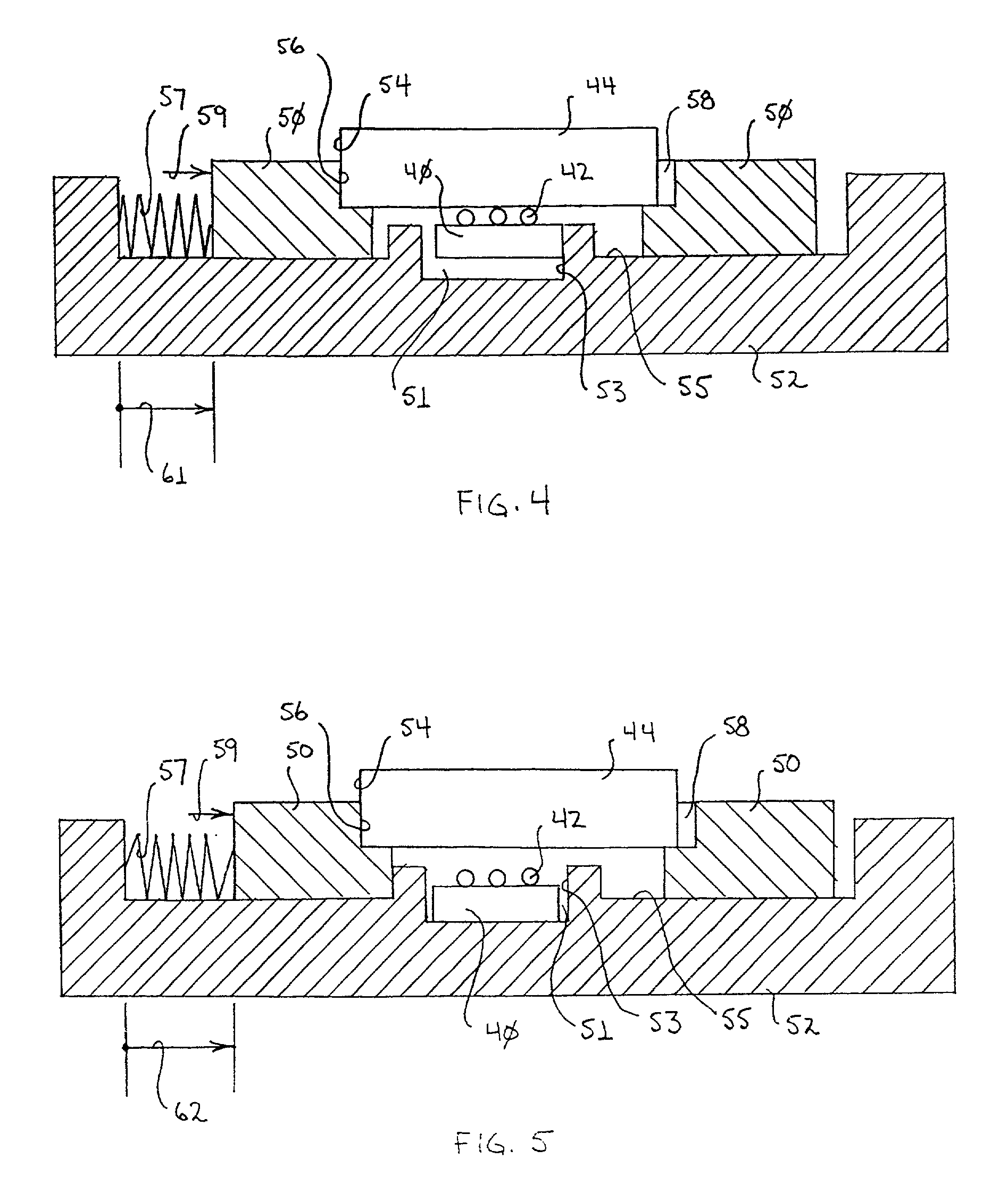
Circuit chips, such as known good die (KGD) chips, are removed from an assembly including a plurality of circuit chips attached to at least one chip carrier, or substrate. The substrate is held within a top plate with the circuit chips positioned within successive chip cavities within a bottom plate. Each chip cavity includes a load surface separated by a cascade effect pitch with respect to adjacent chip cavities. A cascade effect shear force is sequentially applied to the circuit chips to remove them from the substrate. The chips may be heated to a temperature facilitating shear within a temperature range at which solder connections are solid, and the chips further heated following disassembly to a temperature at which the solder is liquid to facilitate reforming the solder for subsequent attachment of the chip into an electronic device.
Description
1. 1. Technical Field of the Invention2. This invention pertains to an apparatus and method for removing soldered electronic components from a substrate. More particularly, it relates to non-destructive, low stress removal of chips temporarily soldered to a substrate during Known-Good-Die (KGD) processing of flip chip devices.3. 2. Background Art4. As technology has evolved, semiconductor devices have become smaller and more dense, which has resulted in corresponding increases in overall chip failure rates, which in turn results in uncompetitive situations for chip manufacturers. In order to readily identify and eliminate the use of defective chips before the defective chips are finally mounted in a product, burn-in processes have evolved. During the burn-in process, normally a chip carrier is provided for testing the chips. The chip carrier has electrical contacts which correspond to the electrical contacts on the semiconductor chip. It is desirable for the carrier contacts to be m...
Claims
Login to View More Application Information
Patent Timeline
 IPC IPC(8): B23K1/018G06F11/26
CPCB23K1/018B23K2201/40G06F11/26B23K2101/40
InventorBERGERON, CHRISTIANLORD, RAYMONDRACICOT, MARIO
OwnerIBM CORP