Negative resistance device

a negative resistance and memory technology, applied in semiconductor devices, digital storage, instruments, etc., can solve the problems of dram memory not matching the speed of the central processor unit (cpu), dram is the least expensive semiconductor memory available, and inconvenient storage and storag

Inactive Publication Date: 2001-06-28
NATIONAL UNIVERSITY OF IRELAND
View PDF0 Cites 72 Cited by
  • Summary
  • Abstract
  • Description
  • Claims
  • Application Information

AI Technical Summary

Problems solved by technology

This capacitor leaks charge with time and hence the memory needs to be periodically refreshed by the peripheral circuitry to retain its memory content.
DRAM memories cannot match the speed of the central processor unit (CPU) due to charging current limits (during memory read/write operations) and destructive reading which necessitates rewrite operation.
However, DRAM is the least expensive semiconductor memory available on the market today and hence is used in most computers as the core memory.
However, this added functionality is area-intensive because SRAM memory cells consist of eith

Method used


Image

  • Negative resistance device
  • Negative resistance device
  • Negative resistance device

Examples


Embodiment Construction

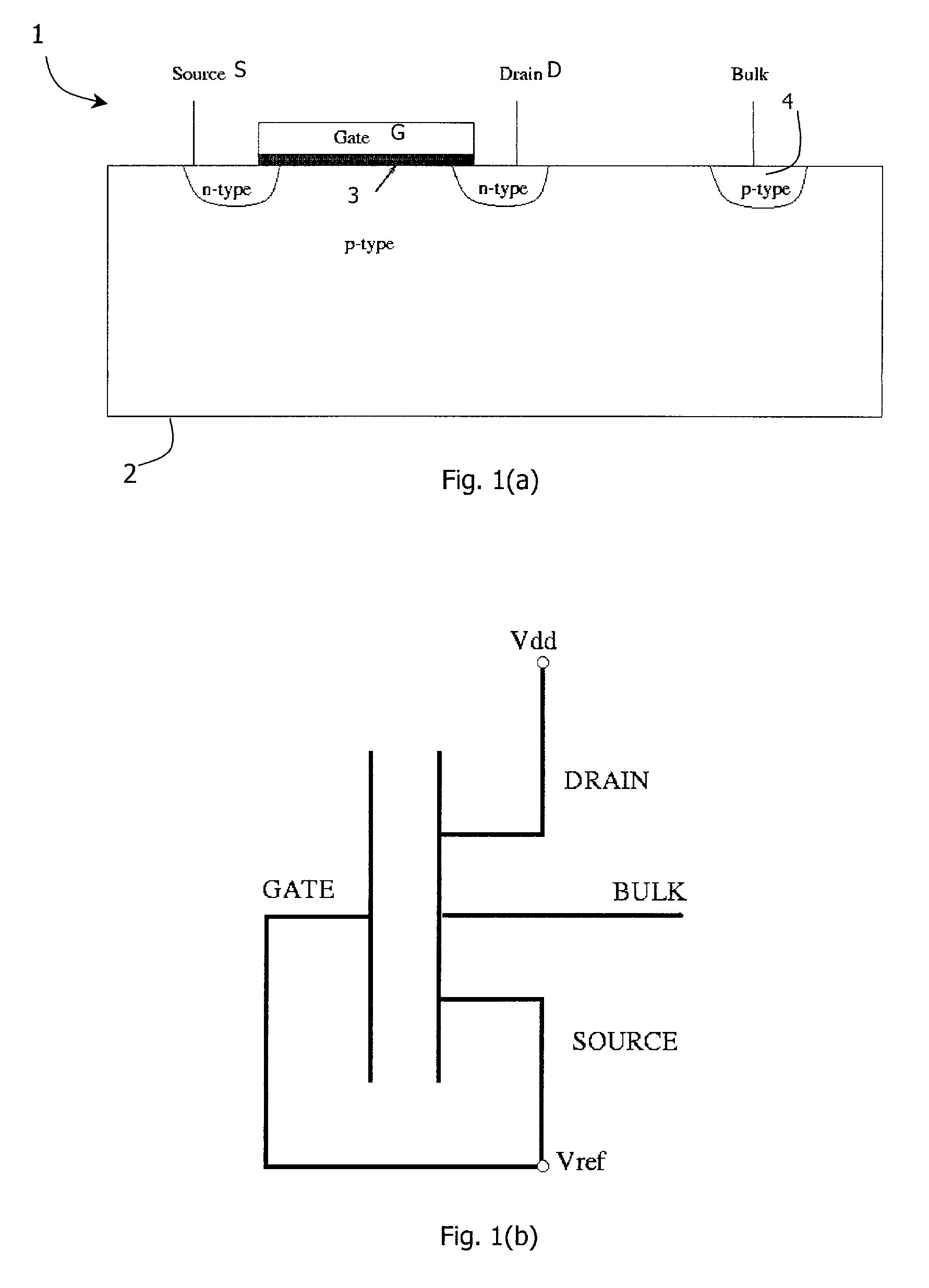
[0039] Referring to FIGS. 1(a) and 1(b), a negative resistance device (NRD), of the invention comprises a MOSFET structure 1 and a bias means, not shown. In this embodiment, the device has a p-type bulk region, however, it may alternatively have an n-type bulk region with appropriate changes to the polarity of the dopants in the structure and the applied biases. Of course, for an n-type bulk region the word "positive" should be replaced with the word "negative" in the following description.

[0040] The NRD physical structure is similar to that of a MOSFET. It comprises a bulk 2 of p-type material and source (S) and drain (D) regions of n-type material fully or partially contained in the bulk. A gate region G of n type polysilicon is insulated from the bulk by a dielectric material 3 of silicon dioxide material. The gate region G extends over the source S and the bulk 2 which includes the junction between the bulk and the source regions. The structure 1 also comprises a bulk terminal 4...


PUM


Abstract

A negative resistance device (NRD) has a MOSFET-like structure, and is biased by: shorting the gate and source together at a fixed applied potential and applying a different fixed potential to the drain, and sweeping the bulk potential towards the drain potential, causing the bulk current to exhibit a negative resistance characteristic. The NRD may be used in a memory circuit (10) in which a resistor (R) is connected between the bulk (2) and a fixed potential. Two States of the circuit at which the current through the resistor matches that through the bulk of the NRD are stable, providing for bistable memory operation.

Description

[0001] The invention relates to electronic circuit memories.PRIOR ART DISCUSSION[0002] At present, the two primary volatile memory technologies in use are Dynamic Random Access Memory (DRAM) and Static Random Access Memory (SRAM).[0003] Dynamic Random Access Memory (DRAM) is a volatile random-access memory that stores information as a charge on a capacitor. This capacitor leaks charge with time and hence the memory needs to be periodically refreshed by the peripheral circuitry to retain its memory content. DRAM memories cannot match the speed of the central processor unit (CPU) due to charging current limits (during memory read / write operations) and destructive reading which necessitates rewrite operation. However, DRAM is the least expensive semiconductor memory available on the market today and hence is used in most computers as the core memory. DRAM cells consist of one transistor and one capacitor.[0004] Static Random Access Memory (SRAM) is as fast as the CPU and is capable of ...

Claims


Application Information

Patent Timeline
IPC IPC(8): G11C5/14G11C11/39G11C11/40H01L27/00
CPCG11C5/142G11C11/39G11C2211/5614
Inventor DUANE, RUSSELLMATHEWSON, ALANCONCANNON, ANN
Owner NATIONAL UNIVERSITY OF IRELAND
Why Eureka
Try Eureka