This helps you quickly interpret patents by identifying the three key elements:
Problems solved by technology
Method used
Benefits of technology
Benefits of technology
[0008] To achieve the above-stated object, a method of forming a gate oxide layer according to the invention is provided. In the method, a furnace or rapid thermal oxidation (RTO) chamber where a semiconductor substrate having a native oxide layer formed thereon is located is supplied with a high-temperature hydrogen gas to deoxidize the native oxide layer. Then, a gate oxide layer is formed over the semiconductor substrate. The semiconductor substrate having the gate oxide layer formed thereon is transferred through a vacuum transmission system into a reaction chamber where a polysilicon layer is formed on the gate oxide layer. Thus, the semiconductor substrate can avoid exposure to an oxygen-containing atmosphere to re-form a native oxide layer thereon.
[0009] Additionally, to achieve the above-stated object, a method of forming a gate oxide layer according to the invention is provided. In the method, a semiconductor substrate already having a native oxide layer formed thereon is oxidized to form a gate oxide layer beneath the native oxide layer. In the same system, the native oxide layer is deoxidized by supplying a high-temperature hydrogen gas. Next, the semiconductor substrate having the gate oxide layer formed thereon is transferred to a reaction chamber through a vacuum transmission system for the formation of a polysilicon gate. Thus, the semiconductor substrate can avoid exposure to an oxygen-containing atmosphere to re-form a native oxide layer thereon.
Problems solved by technology
In very large semiconductor integration (VLSI) process, the thickness of a gate oxide layer of an MOS (MetalOxideSemiconductor) device is approximately 100-200.ANG.. For a high-level device, such as a flash memory, the thickness of a tunneling oxide layer is less than 100.ANG., even approximately 30.ANG.. Thus, it is very difficult to form a high-quality gate oxide layer with such a thin thickness.
In addition to the problem of uneasy controlling the quality of a gate oxide layer formed with such a thin thickness, it has to overcome influences brought by a native oxide layer with a thickness of approximately 2-10.ANG. which still remains after a pre-cleaning step and before the formation of the gate oxide layer.
After that, subsequent oxidation becomes more difficult since reaction-participating oxygen molecules must first reach the surface of the silicon dioxide layer, and then diffuse therein onto the surface of the siliconwafer for oxidation.
Furthermore, the native oxide layer with a poor uniformity can affect the quality of a subsequently formed gate oxide layer.
Therefore, how to avoid the formation of the native oxide layer or eliminate the native oxide layer becomes a very important issue.
Moreover, a gate oxide layer is formed beneath the native oxide layer, such that when a patterned polysilicon layer, serving as a gate structure, is formed on the native oxide layer, water molecules adhere to the native oxide layer, lowering the reliability of the gate structure.
Method used
Image
Click on the blue label to locate the original text in one second.
Reading with bidirectional positioning of images and text.
Examples
embodiment 1
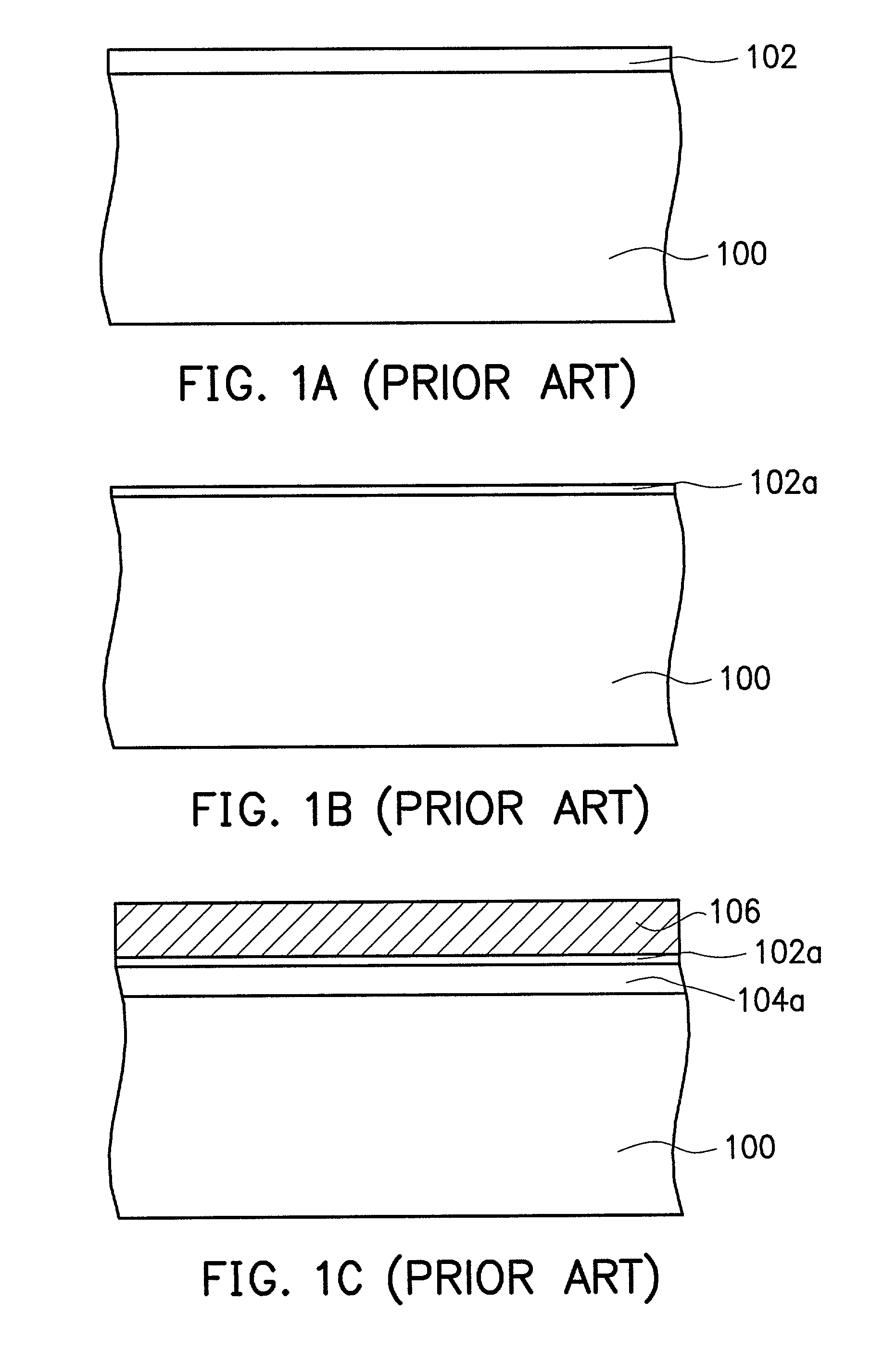
[0013] FIGS. 1A-1C are schematic cross-sectional views showing a method of forming a gate oxide layer after deoxidizing a native oxide layer according to a first preferred embodiment of the invention.
[0014] Referring to FIG. 1A, a semiconductor substrate 100 is first rinsed so as to remove impurities and part of a native oxide layer (not shown) naturally formed thereon in an oxygen-containing atmosphere. After that, a native oxide layer 102 with a thickness of approximately 2-10.ANG. remains on the semiconductor substrate 100.
[0015] Referring to FIG. 1B, the semiconductor substrate 100 is sent into, for example, a furnace, which is supplied with a high-temperature hydrogen gas having a temperature of approximately 750-900.degree. C. and a flow of 0.5-5 sccm. With the high-temperature hydrogen gas, the native oxide layer 102 is partly deoxidized to form a remaining native oxide layer 102a, or even completely deoxidized.
[0016] Referring to FIG. 1C, a gate oxide layer 104a with a thick...
embodiment 2
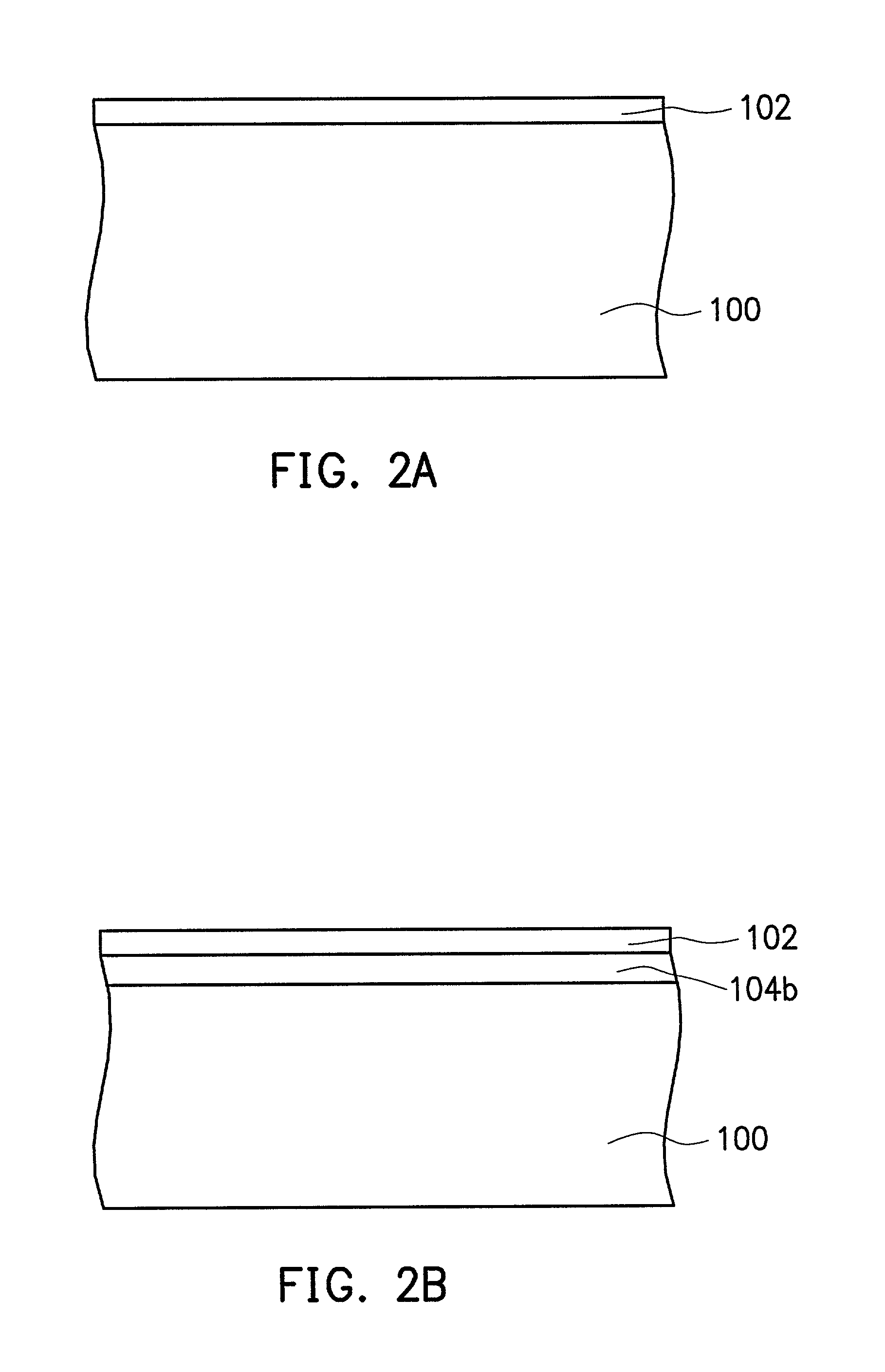
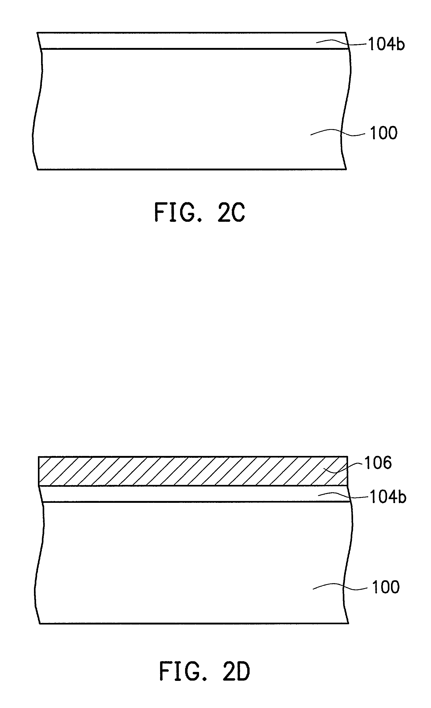
[0017] FIGS. 2A-2D are schematic, cross-sectional views showing a method of forming a gate oxide layer before deoxidizing a native oxide layer according to a second preferred embodiment of the invention.
[0018] Referring to FIG. 2A, a semiconductor substrate 100 is first rinsed so as to remove impurities and part of a native oxide layer (not shown) naturally formed thereon in an oxygen-containing atmosphere. After that, a native oxide layer 102 with a thickness of approximately 2-10.ANG. remains on the semiconductor substrate 100.
[0019] Referring to FIG. 2B, a gate oxide layer 104b with a thickness of approximately 30.ANG. is formed between the substrate 100 and the native oxide layer 102 in, for example, a rapid thermal oxidation chamber, a furnace or the like.
[0020] Referring to FIG. 2C, the semiconductor substrate is sent into, for example, a furnace, which is supplied with a high-temperature hydrogen gas having a temperature of approximately 750-900.degree. C. and a flow of 0.5-5...
PUM
Abstract
A method of forming a gate oxide layer according to the invention is disclosed. In the method, a furnace or rapid thermal oxidation (RTO) chamber where a semiconductor substrate having a native oxide layer formed thereon is located is supplied with a high-temperature hydrogen gas to deoxidize the native oxide layer. Then, a gate oxide layer is formed over the semiconductor substrate. The semiconductor substrate having the gate oxide layer formed thereon is transferred through a vacuum transmission system into a reaction chamber where a polysilicon layer is formed on the gate oxide layer. Thus, the semiconductor substrate can avoid exposure to an oxygen-containing atmosphere to re-form a native oxide layer thereon.
Description
BACKGROUND OF THE INVENTION[0001] 1. Field of the Invention[0002] The invention relates to a method of forming a semiconductor device, and in particular to a method of forming a high-quality gate oxide layer by deoxidizing a native oxide.[0003] 2. Description of the Related Art[0004] In very large semiconductor integration (VLSI) process, the thickness of a gate oxide layer of an MOS (MetalOxideSemiconductor) device is approximately 100-200.ANG.. For a high-level device, such as a flash memory, the thickness of a tunneling oxide layer is less than 100.ANG., even approximately 30.ANG.. Thus, it is very difficult to form a high-quality gate oxide layer with such a thin thickness. In addition to the problem of uneasy controlling the quality of a gate oxide layer formed with such a thin thickness, it has to overcome influences brought by a native oxide layer with a thickness of approximately 2-10.ANG. which still remains after a pre-cleaning step and before the formation of the gate o...
Claims
Application Information
Patent Timeline
Application Date:The date an application was filed.
Publication Date:The date a patent or application was officially published.
First Publication Date:The earliest publication date of a patent with the same application number.
Issue Date:Publication date of the patent grant document.
PCT Entry Date:The Entry date of PCT National Phase.
Estimated Expiry Date:The statutory expiry date of a patent right according to the Patent Law, and it is the longest term of protection that the patent right can achieve without the termination of the patent right due to other reasons(Term extension factor has been taken into account ).
Invalid Date:Actual expiry date is based on effective date or publication date of legal transaction data of invalid patent.

