

Method of manufacturing semiconductor device
a manufacturing method and semiconductor technology, applied in the direction of semiconductor devices, electrical devices, transistors, etc., can solve the problems of dummy side wall, dummy side wall, and dummy side wall, and achieve rapid thermal oxidation, high quality, and high quality
- Summary
- Abstract
- Description
- Claims
- Application Information
AI Technical Summary
Benefits of technology
Problems solved by technology
Method used
Image

Examples
first embodiment
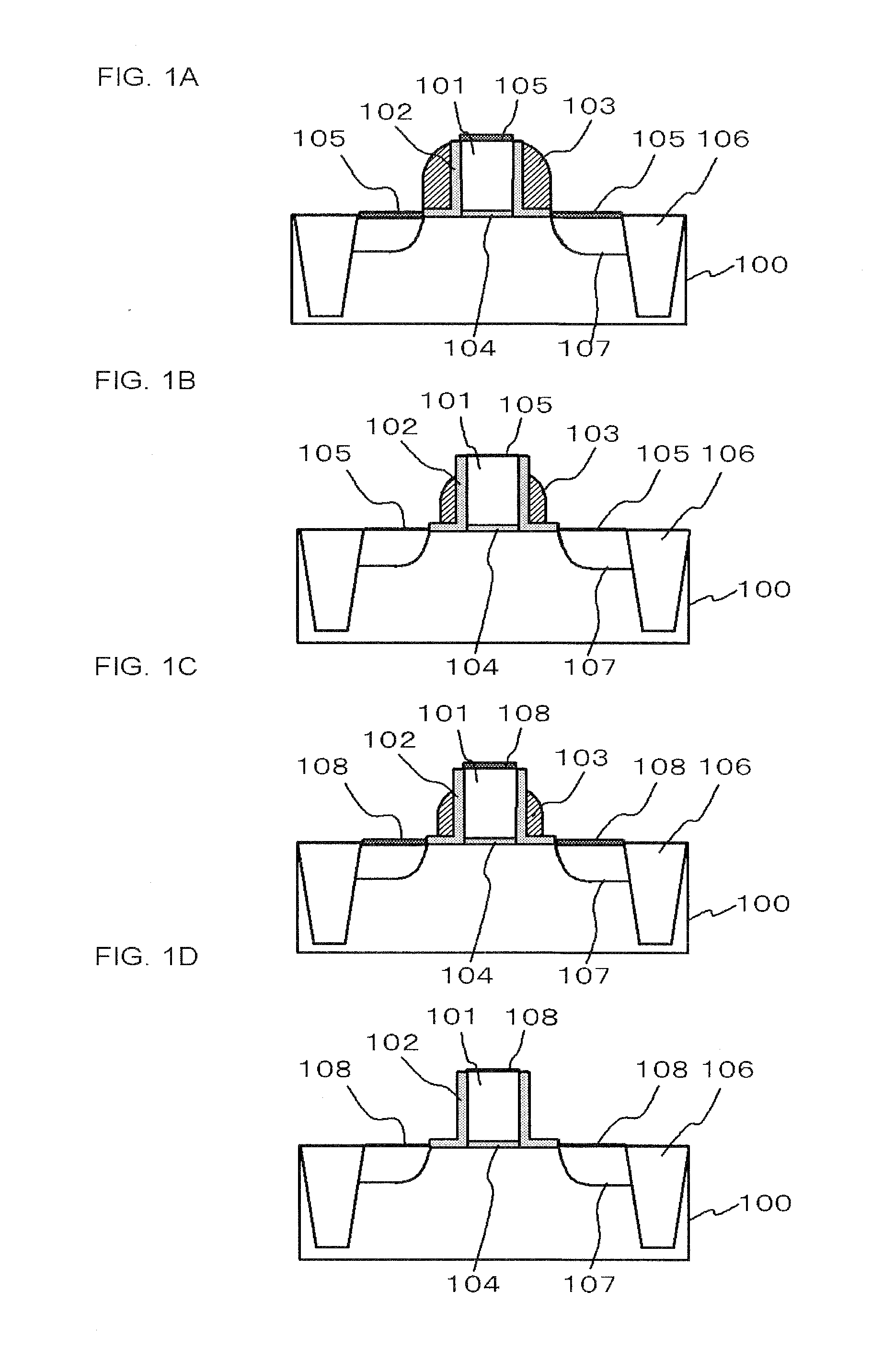
[0040]In the present embodiment, an exemplary implementation of removing a dummy side wall formed on a side surface of a gate electrode and serving as a mask for doping an impurity to form a source-drain region after doping the impurity will be described.
[0041]FIGS. 1A to 1D and FIGS. 2A to 2D are cross-sectional views, sequentially showing a process for manufacturing a semiconductor device in first embodiment of the present invention.
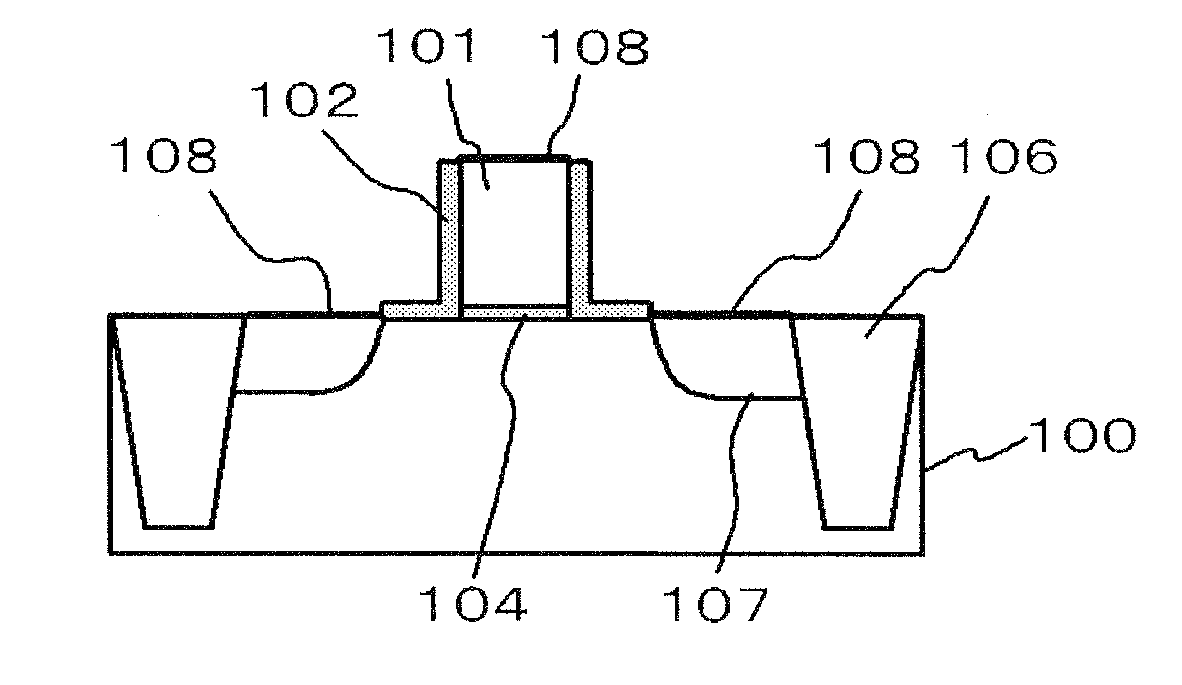
[0042]First of all, as shown in FIG. 1A, a gate insulating film 104 and a gate electrode 101 composed of polysilicon are formed on a silicon substrate 100 having an oxide film 106 for element isolation formed thereon, and then a dummy side wall 103 (first film) is formed on both side surfaces of the gate electrode 101 through a dummy oxide film 102 therebetween, and further an ion-implanting is performed on both sides of the dummy side wall 103 and an activation annealing is performed to form the source-drain region 107. The dummy side wall 103 is form...
second embodiment
[0056]In the present embodiment, an exemplary implementation for removing a hard mask during the processing of the gate electrode will be described.
[0057]FIGS. 5A to SD are cross-sectional views, sequentially showing a process for manufacturing a semiconductor device in second embodiment of the present invention. A gate electrode film composed of a gate insulating film 204 and a polysilicon is deposited on a silicon substrate 200 having an oxide film 206 for element isolation formed thereon, and a hard mask 203 (first film) having a geometry equivalent to a gate electrode geometry is formed on the gate electrode film. The gate electrode film and the gate insulating film 204 are etched to form a gate electrode 201. Here, the hard mask 203 is formed of a film containing nitrogen. More specifically, the film is a silicon nitride film.
[0058]Next, polysilicon on both side surfaces of the silicon substrate 200 and the gate electrode 201 are oxidized to form the first silicon oxide film 20...
example 1
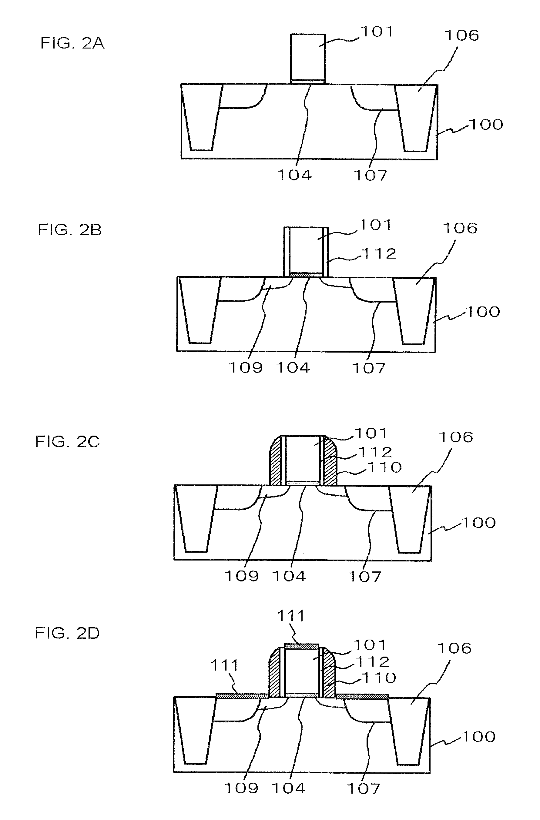
[0069]Specimens were prepared in accordance with the first embodiment as shown with FIGS. 1A to 1D and FIGS. 2A to 2D. More specifically, the gate electrode 101 was formed on the silicon substrate 100 with the gate insulating film 104 (having film thickness of 1.0 to 1.5 nm) and polysilicon doped with phosphorus, and the dummy side wall 103 (first film) was formed on the gate electrode 101 through the dummy oxide film 102, and then an ion-implanting was performed on both sides of the dummy side wall 103 and an activation annealing is performed to form the source-drain region 107. Thereafter, an impurity was doped into the extension region 109, and then a silicide 111 was formed to provide a transistor. A specimen 1 is manufactured by the method of manufacturing the semiconductor device of first embodiment, and specimens 2, 3 and 4 are manufactured by the method for the semiconductor device as illustrated in the above description shown in FIGS. 3A to 3D and FIGS. 4A and 4B.
[0070]The ...
PUM
| Property | Measurement | Unit |
|---|---|---|
| thickness | aaaaa | aaaaa |
| thickness | aaaaa | aaaaa |
| thick | aaaaa | aaaaa |
Abstract
Description
Claims
Application Information