Fabrication method of submicron gate using anisotropic etching

a technology of anisotropic etching and submicron gate, which is applied in the direction of semiconductor devices, electrical apparatus, transistors, etc., can solve the problems of increased manufacturing costs, high cost, and high exposure process requirements, and achieve the effect of reducing the distance between the base and the base resistan

Inactive Publication Date: 2001-10-04
KOREA ADVANCED INST OF SCI & TECH
View PDF0 Cites 50 Cited by
  • Summary
  • Abstract
  • Description
  • Claims
  • Application Information

AI Technical Summary

Benefits of technology

0014] In the formation of a base electrode involved in the fabrication of an HBT device, the present invention also provides an effect of reducing the distance betw

Problems solved by technology

However, these techniques require an expensive exposure process, such as an electron beam writing process or a stepped exposure process, to form a submicron gate.
However, this technique requires an expensive exposure process, such as

Method used


Image

  • Fabrication method of submicron gate using anisotropic etching
  • Fabrication method of submicron gate using anisotropic etching
  • Fabrication method of submicron gate using anisotropic etching

Examples


Embodiment Construction

[0025] Now, a preferred embodiment of the present invention will be described in detail, with reference to the annexed drawings.

[0026] FIGS. 1 to 9 illustrate sequential steps of a submicron gate fabrication and self-alignment procedure according to an embodiment of the present invention, respectively.

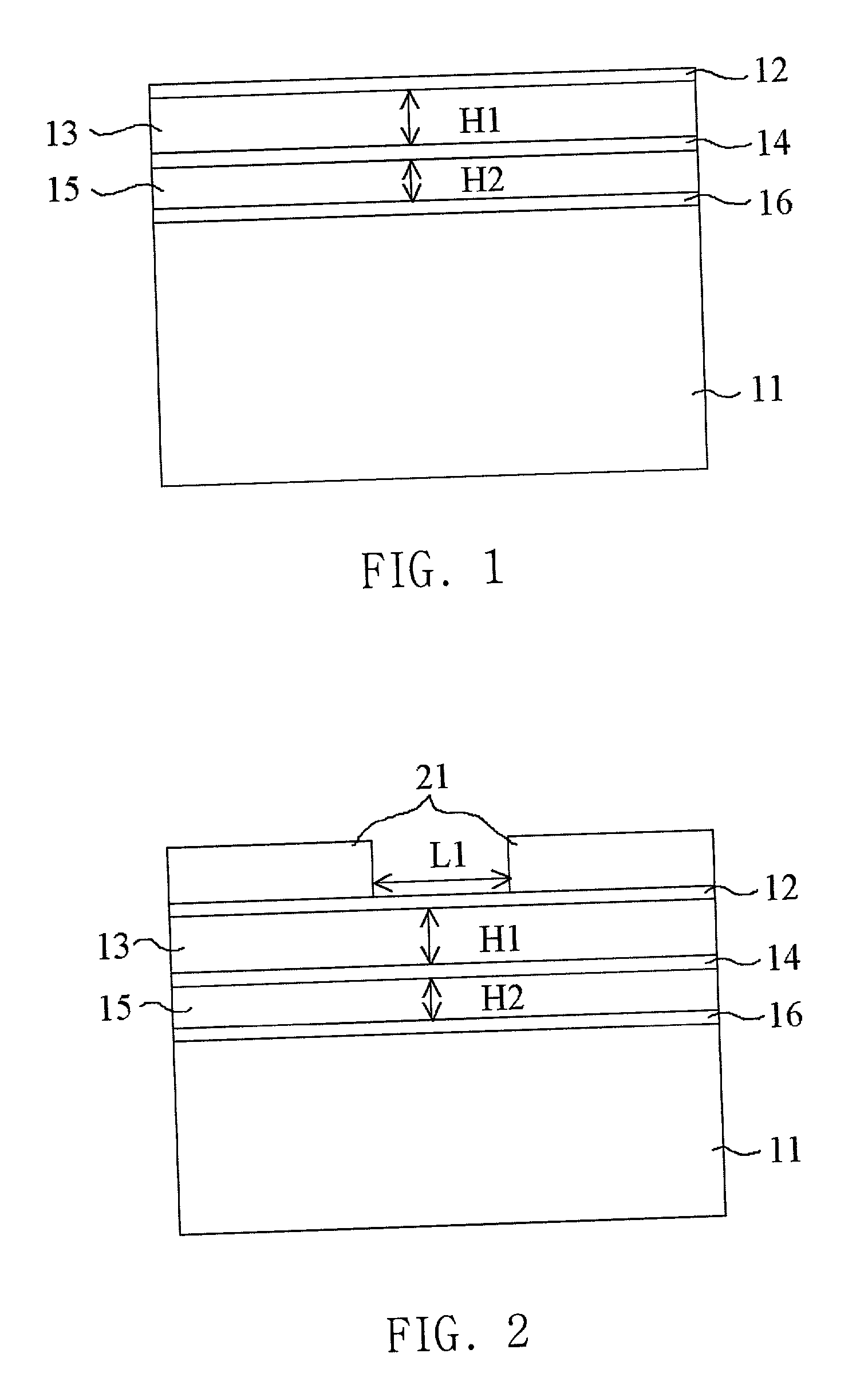
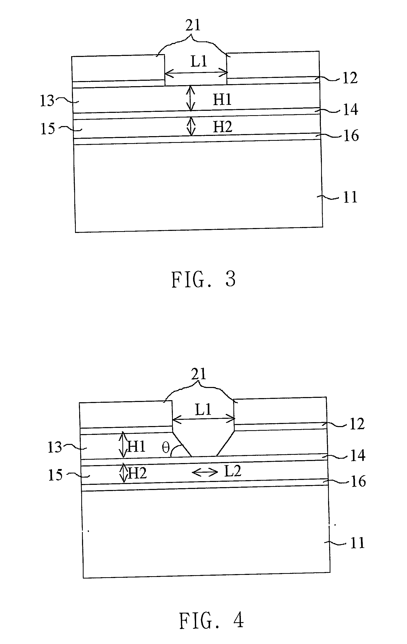
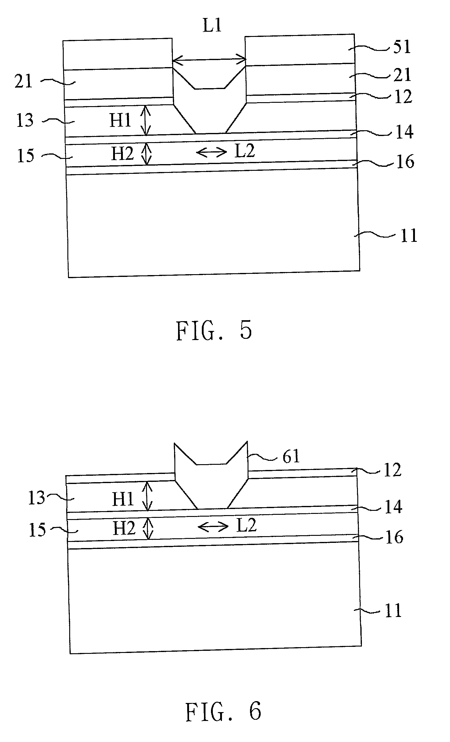
[0027] FIG. 1 illustrates an essential laminated structure according to the embodiment of the present invention in which a dummy emitter is laminated on a general InP / InGaAs heterojunction bipolar transistor (HBT) structure. As shown in FIG. 1, this structure is formed by laminating InGaAs layers (12, 14, and 16), and InP layers (13 and 15) over a Fe-doped InP substrate (11) in an alternating fashion, using a laminated growth equipment such as MOCVD or MBE.

[0028] The second InP layer (15) defines an emitter region, the second InGaAs layer (14) an emitter cap region, and the third InGaAs layer (16) a base region, respectively. The first InGaAs layer (12) and the first InP layer (13) def...


PUM


Abstract

Disclosed is a method for fabricating a self-aligned submicron gate electrode using an anisotropic etching process. The method involves the steps of laminating a dummy emitter defining a dummy emitter region over a heterojunction bipolar transistor structure including layers sequentially formed over a semiconductor substrate to define a base region, an emitter region, and an emitter cap region, respectively, defining a line having a width of about 1 micron on the dummy emitter by use of a photoresist while using a contact aligner, selectively anisotropic etching the dummy emitter at a region where the line is defined, to allow the dummy emitter to have an etched portion having a bottom surface with a width less than the width of the line defined by the photoresist, and depositing a contact metal on the etched portion of the dummy emitter, thereby forming a gate. In accordance with the present invention, a reliable submicron gate can be fabricated using a simple anisotropic wet etch process and an inexpensive contact aligner. Accordingly, the manufacturing costs can be reduced. In the formation of a base electrode involved in the fabrication of an HBT device, the present invention also provides an effect of reducing the distance between a base and an emitter, thereby achieving a reduction in base resistance, by virtue of a self-alignment using a V-shaped submicron gate.

Description

BACKGROUND OF THE INVENTION[0001] 1. Field of the Invention[0002] The present invention relates to a submicron gate electrode of a semiconductor device, and more particularly to a method for fabricating a self-aligned submicron gate electrode using an anisotropic etching process.[0003] 2. Description of the Related Art[0004] Remarkable development recently made in radio communication fields has resulted in an increased demand for ultrahigh broadband communication networks. An exemplary one of such networks is a network for local multipoint distribution services in which audio, video conference, and digital signals are simultaneously transmitted at a bandwidth of 1.3 GHz within a service area of 2 to 7 Km in radius, using a 28 GHz "Ka-band". In order to construct such an ultrahigh broadband communication network, it is very important to develop ultrahigh-frequency devices operating the above mentioned frequency band while achieving a miniature and high performance of devices. To this...

Claims


Application Information

Patent Timeline
IPC IPC(8): H01L21/3213H01L21/331H01L21/28H01L29/417H01L29/73H01L29/737
CPCH01L29/66318H01L21/3213
Inventor KIM, MOON JUNGYANG, KYOUNG HOONKWON, YOUNG SE
Owner KOREA ADVANCED INST OF SCI & TECH
Why Eureka
Try Eureka