Method for direct attachment of a chip to a cooling member

a cooling member and chip technology, applied in the direction of adhesive processes, layered products, chemical instruments and processes, etc., can solve the problems of irrecoverable module yield loss, insufficient process improvement alone to eliminate all the problems affecting both performance and reliability, and insufficient heat flow, etc., to achieve steady state operation of the semiconductor chip, the effect of sufficient bond strength

Inactive Publication Date: 2001-11-15
IBM CORP
View PDF0 Cites 29 Cited by
  • Summary
  • Abstract
  • Description
  • Claims
  • Application Information

AI Technical Summary

Benefits of technology

0018] The above and other objects, which will be apparent to those skilled in the art, are achieved in the present invention which provides in one aspect a chip assembly comprising a substrate having an upper surface for carrying one or more semiconductor chips, at least one semiconductor chip mounted on the upper surface of the substrate and a cap covering the semiconductor chip and the

Problems solved by technology

Semiconductor devices are continually becoming smaller and more dense with the evolution of new technology.
Whereas significant improvements are being made to eliminate systematic problems by reducing process variability, process improvements alone are not sufficient to eliminate all the problems which affect both performance and reliability.
It is well known that a leak in cap 11' may result in irrecoverable module yield losses and degrade expected reliability performance under actual use conditions.
Furthermore, the presence of cap 11' adds additional weight to the completed or assembled module.
This leads to high internal pre

Method used


Image

  • Method for direct attachment of a chip to a cooling member
  • Method for direct attachment of a chip to a cooling member
  • Method for direct attachment of a chip to a cooling member

Examples


Embodiment Construction

)

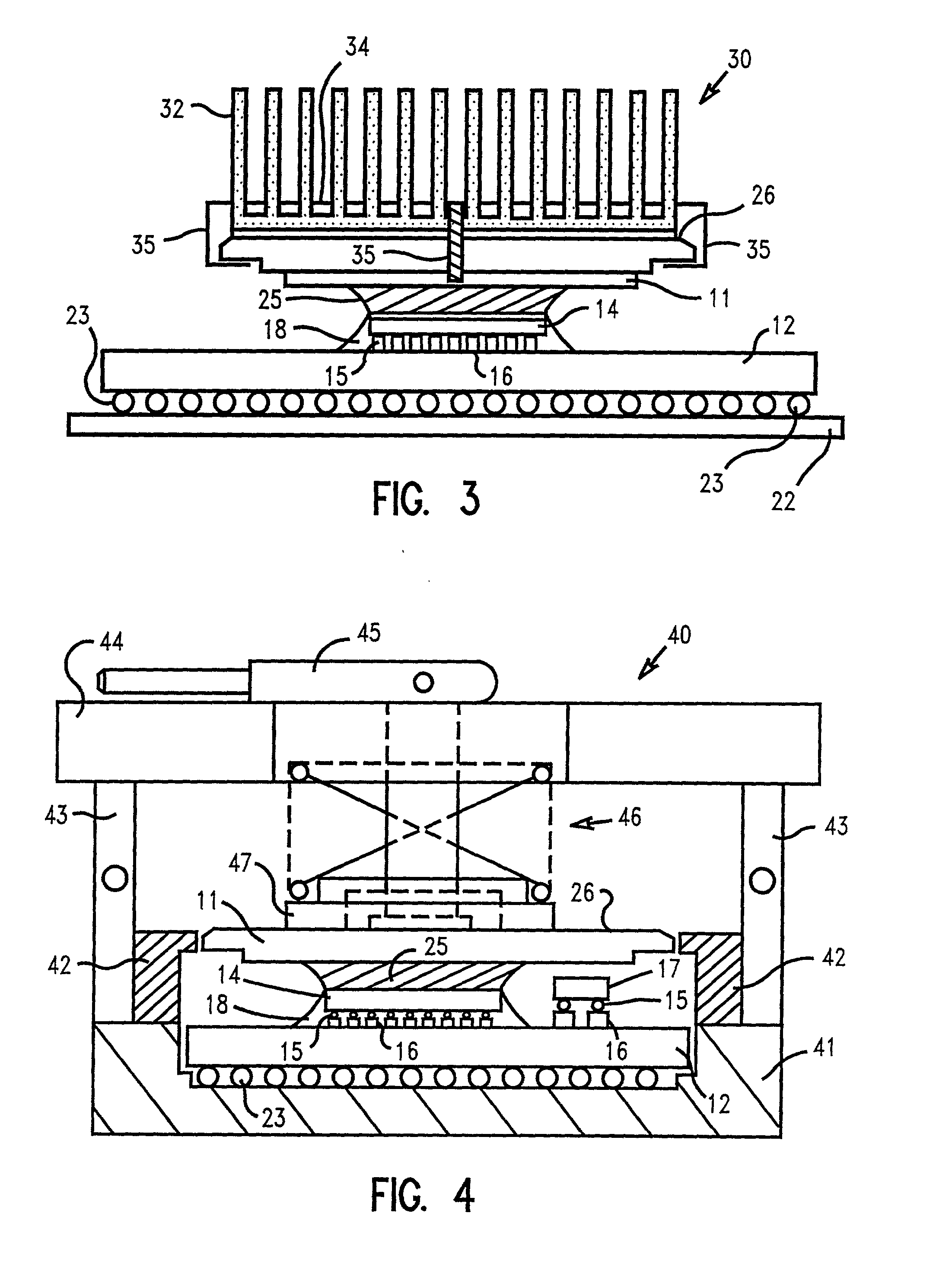
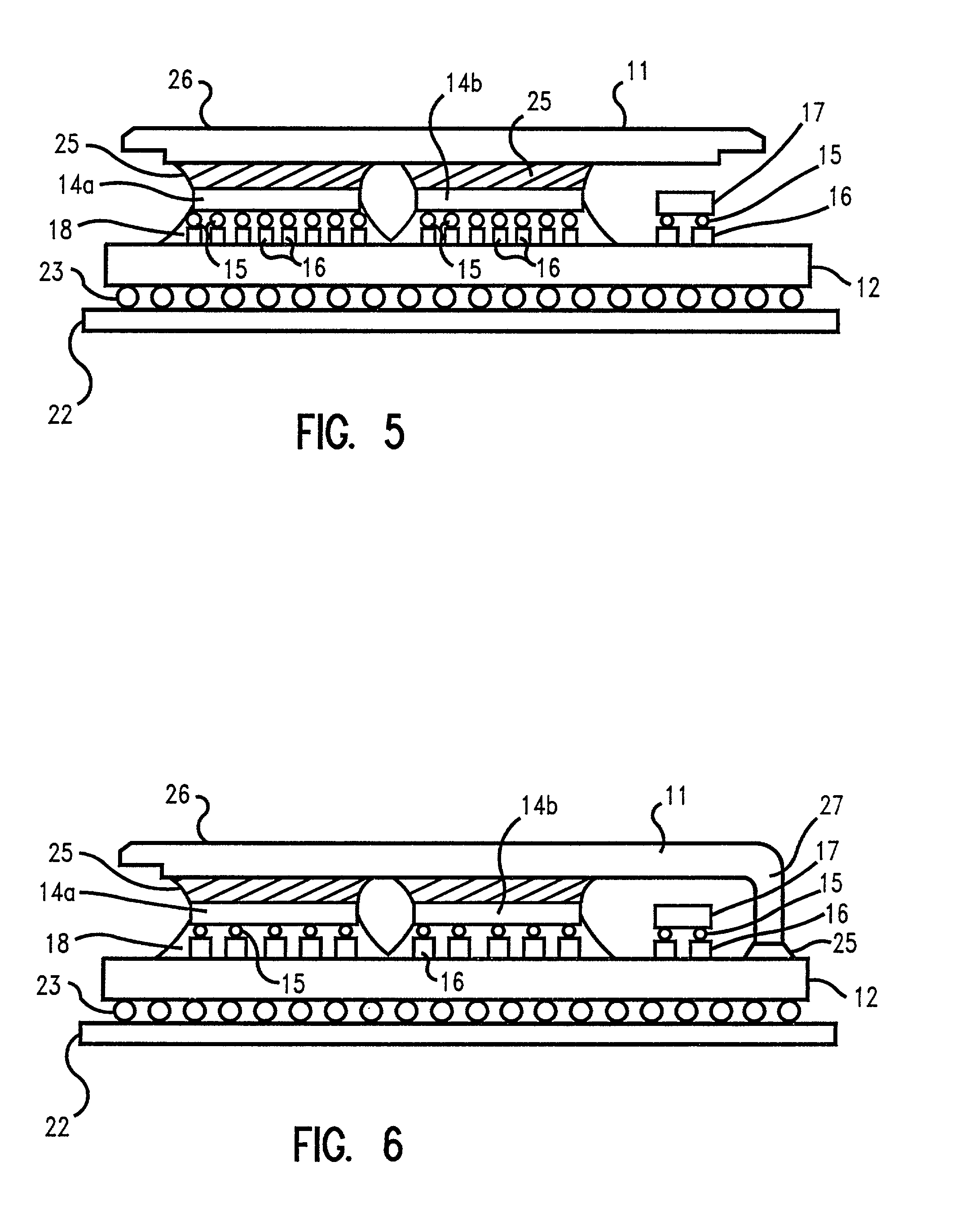
[0035] In describing the preferred embodiment of the present invention, reference will be made herein to FIGS. 1-8 of the drawings in which like numerals refer to like features of the invention. Features of the invention are not necessarily shown to scale in the drawings.

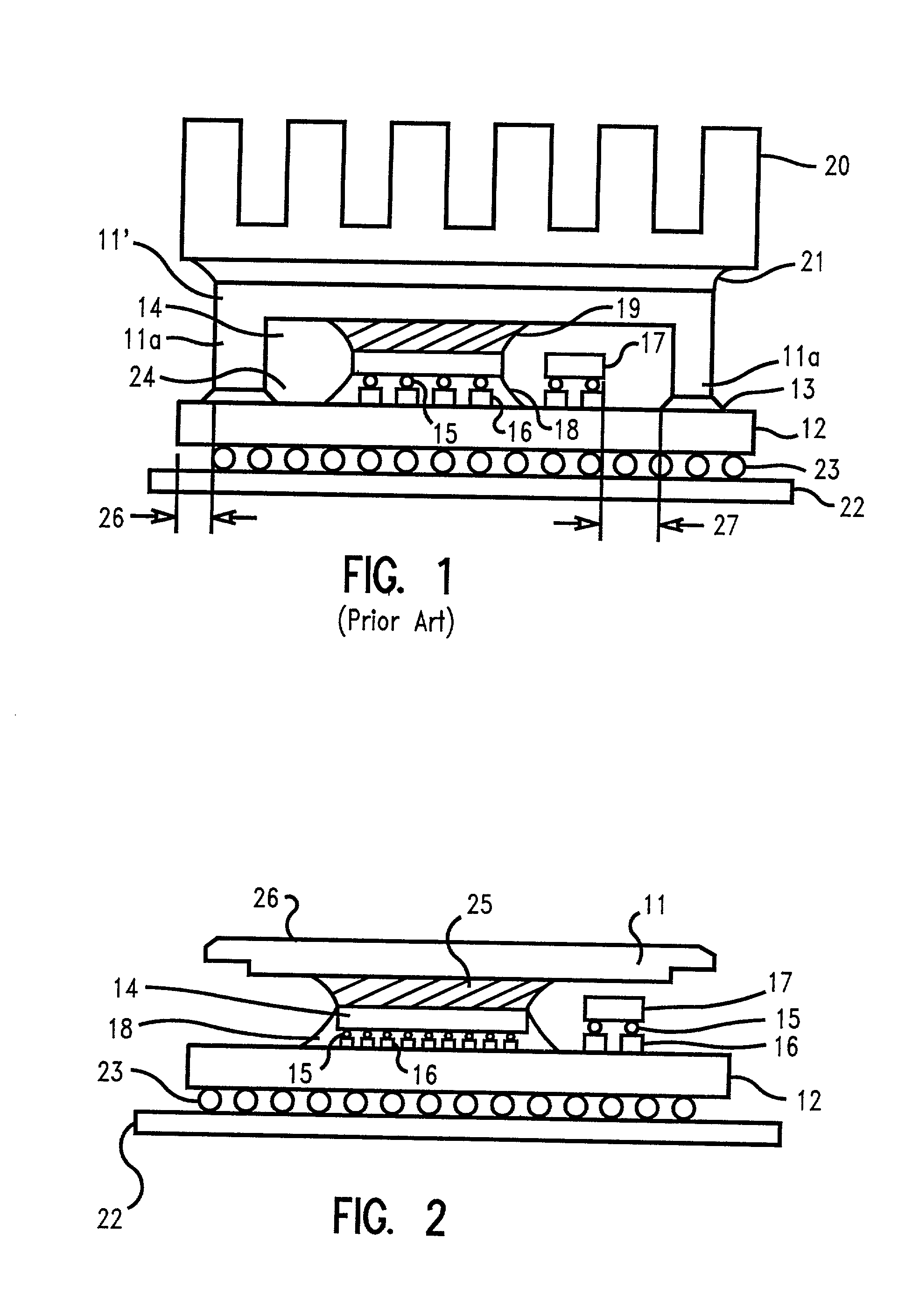
[0036] Designers of ceramic chip carries are under ever increasing pressure to maximize the utilization of available top surface design space to package electronic components, giving the highest regard to cost and space efficiency. This invention describes one way to reduce cost of such packages without any loss or degradation of their performance. Packaging methods which reduce cost advantageously increase the availability of such electronic packages in the marketplace.

[0037] FIG. 2 illustrates a preferred embodiment of the present invention. Ceramic semiconductor chip 14 is connected to substrate 12 by solder balls 15 on pads 16. Chip underfill material 18 encapsulates at least a portion, and preferably all, of s...


PUM

PropertyMeasurementUnit
Massaaaaaaaaaa
Thicknessaaaaaaaaaa
Electrical conductoraaaaaaaaaa

Abstract

A semiconductor chip module uses a silicone adhesive between the semiconductor chip and a cap, said adhesive having sufficient bond strength to secure said cap to said chip without additional mechanical constraint while providing a direct thermally conductive path and permitting sufficient heat flow from said chip to said cap to maintain steady state operation of said semiconductor chip. The preferred silicone adhesive comprises a primerless, two-part polysiloxane-based adhesive made by reacting polydimethyl siloxane, an organosilicon compound, a polysiloxane, and a silane, in the presence of a catalyst.

Description

[0001] 1. Field of the Invention[0002] The present invention relates generally to a semiconductor chip assembly and, in particular, to an apparatus that uses a flexible, silicone elastomer adhesive to directly join a chip or plurality of chips to one or several cooling members.[0003] 2. Description of Related Art[0004] Semiconductor devices are continually becoming smaller and more dense with the evolution of new technology. However, increases in circuit density produce a corresponding changes in overall chip packaging strategies in order to remain competitive. Chip and chip carrier manufacturers are therefore constantly challenged to improve the quality of their products by identifying and eliminating problems, reducing package size and weight, decreasing package costs and providing improved thermal efficiencies with new generations of advanced devices. Whereas significant improvements are being made to eliminate systematic problems by reducing process variability, process improvem...

Claims


Application Information

Patent Timeline
IPC IPC(8): C08L83/06C09J5/06C09J183/04H01L23/373H01L23/42
CPCC08L83/06H01L2224/73204C09J183/04C09J2483/00H01L23/3737H01L23/42H01L2224/16H01L2224/73253H01L2924/01078H01L2924/15311H01L2924/16152H01L2924/19105C09J5/06H01L2224/32245H01L2224/32225H01L2224/16227H01L2224/16225H01L2924/10253H01L2924/00H01L23/34
Inventor POMPEO, FRANK LOUISCARON, ALAIN A.COFFIN, JEFFREY THOMASZITZ, JEFFREY ALLEN
Owner IBM CORP
Why Eureka
Try Eureka