CVD apparatus

a technology of cvd apparatus and cvd spherical tube, which is applied in the direction of coatings, chemical vapor deposition coatings, adhesives, etc., can solve the problems of increasing parasitic capacitance, increasing wiring resistance, and increasing the time delay of electric signals in the integrated circui

Inactive Publication Date: 2001-11-22
ANELVA CORP
View PDF0 Cites 162 Cited by
  • Summary
  • Abstract
  • Description
  • Claims
  • Application Information

AI Technical Summary

Problems solved by technology

Such reduction in wiring dimensions leads to an increase in wiring resistance and also narrowing of wiring spacing leads to an increase in parasitic capacitance between wirings, which causes a problem that time delay of electric signals in integrated circuits increases.
In this case, a measure to increase a wiring height to increase a cross sectional area of wiring is taken in order to suppress an increase in wiring resistance but a wiring height cannot be increased excessively because the increase in areas of facing surfaces of wirings leads to the increase in parasitic capacitance.
Such problem in time delay of signals has become serious to the extent that the normal operations of integrated circuits are impeded in wiring dimensions of around 0.1 micron.
Also, an increase in resistance and electric current density, due to a reduced wiring width, will cause wiring temperature rise due to Joule heat and electromigration to degrade reliability in integrated circuits.
Meanwhile, w

Method used


Image

  • CVD apparatus
  • CVD apparatus
  • CVD apparatus

Examples


first embodiment

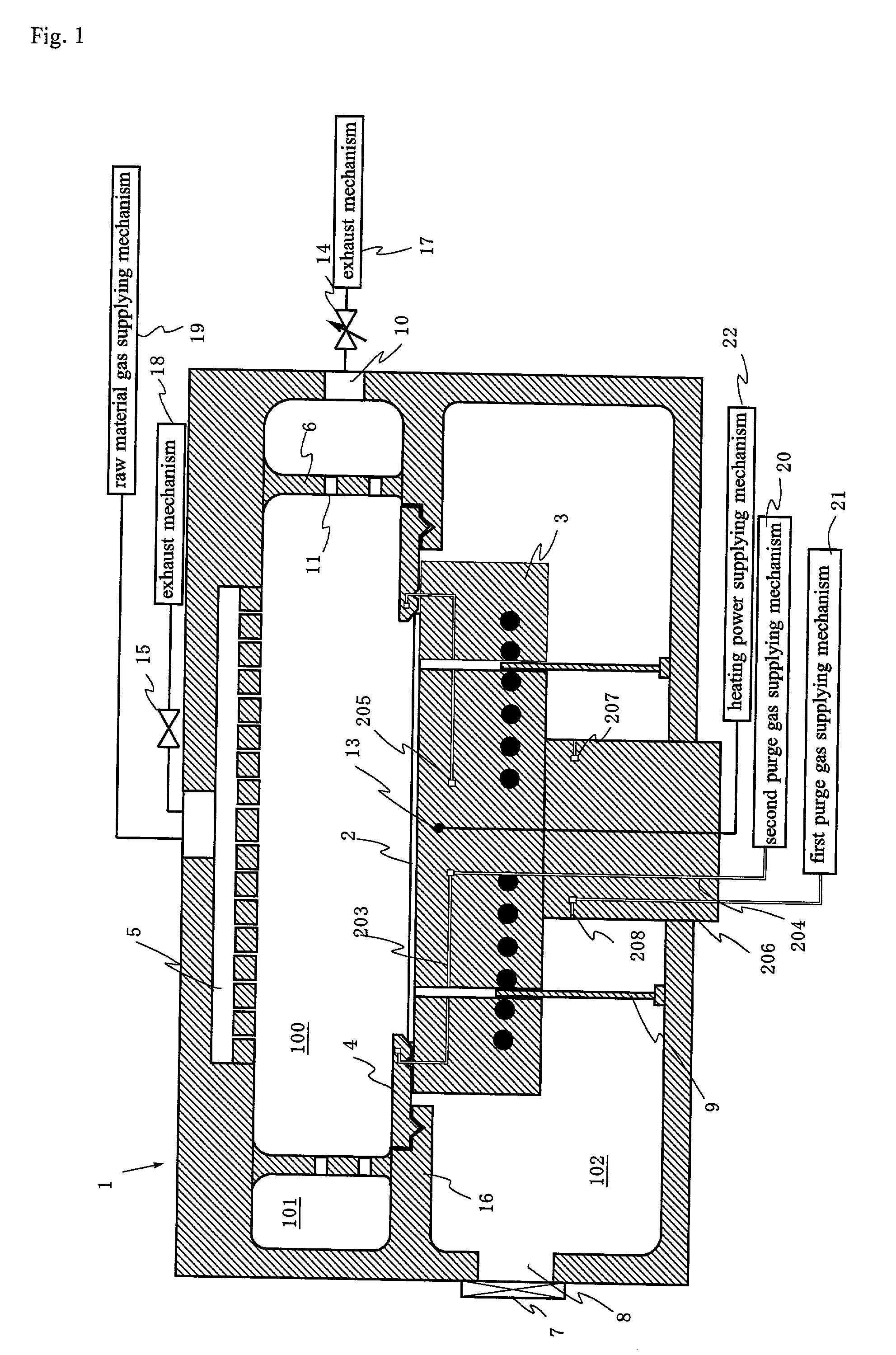
[0052] An exemplary construction of a CVD apparatus according to the invention is shown in a schematic cross sectional view of FIG. 1. FIG. 1 shows an interior of a reduced pressure vessel at the time of deposition. As shown in the figure, the interior of the reduced pressure vessel 1 is divided into three chambers, that is, a deposition chamber 100, an exhaust chamber 101 and a transfer chamber 102, the deposition chamber and the exhaust chamber being arranged above the transfer chamber to be disposed in axial symmetry around the same central axis.

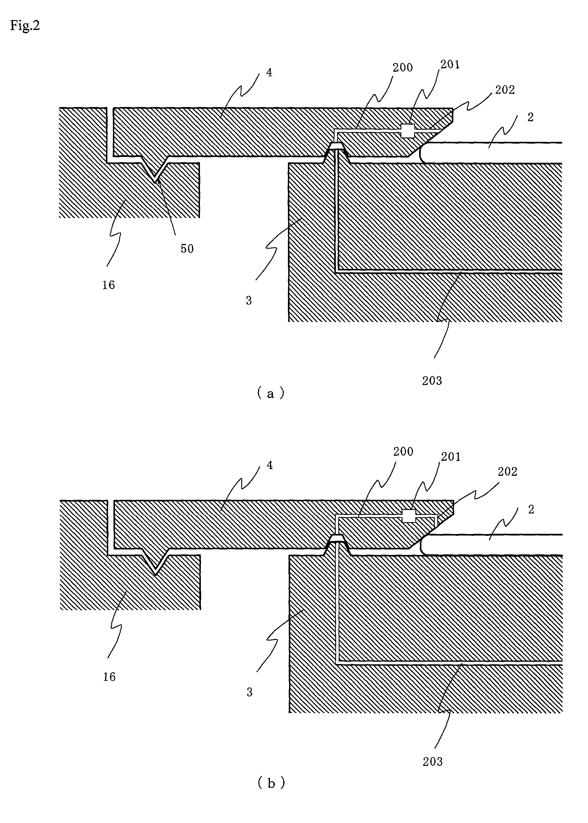
[0053] A substrate 2 is placed on a vertically movable heating holder 3, and a tapered edge formed on the inner circumference end of a doughnut-shaped ring chuck 4 contacts entirely circumferentially with the edge of the substrate 2 to fix the same. A gas introducing section 5 is provided in a position opposed to the substrate to be connected to a raw material gas supplying mechanism 19 outside to introduce into the deposition chamber 100...

second embodiment

[0086] Subsequently, the invention will be described.

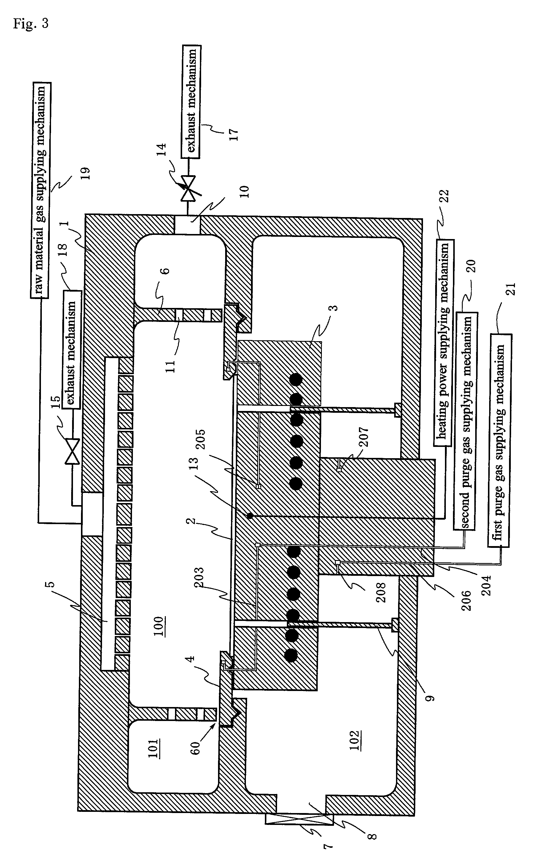
[0087] FIG. 3 is a schematic cross sectional view showing another exemplary construction of a CVD apparatus of the invention. A primary difference between the CVD apparatus of the present embodiment and the CVD apparatus shown in FIG. 1 resides in that an inner wall 6 separating the deposition chamber 100 and the exhaust chamber 101 from each other is mounted in a different position. More specifically, with the CVD apparatus shown in FIG. 3, the inner wall is suspended above the ring chuck 4 from the roof plate of the vessel to leave a predetermined gap 60 between the ring chuck and the inner wall. The deposition chamber 100 and the exhaust chamber 101 are spatially joined to each other by way of the holes 11 provided in the inner wall 6 and the gap 60 between the inner wall 6 and the ring chuck, and the transfer chamber 102 and the exhaust chamber 101 are spatially joined to each other by way of the gap 50 between the ring chuck ...


PUM

PropertyMeasurementUnit
Pressureaaaaaaaaaa
Circumferenceaaaaaaaaaa

Abstract

The present invention is to provide a CVD apparatus having a high productivity, involving less contamination on the back surface of a substrate and having a high yield. A CVD apparatus for forming a thin film is characterized in that the interior of the vessel is divided into a upper portion and a lower portion (transfer chamber) by a support member for holding the ring chuck and the upper portion is further divide by inner wall into a deposition chamber and an exhaust chamber in axial symmetry around the same central axis. The deposition chamber communicated to the exhaust chamber through a gap between the inner wall and the ring chuck and/or holes provided in the inner wall. The transfer chamber is communicated to the deposition chamber or exhaust chamber through a gap formed between the ring chuck and the support member.

Description

[0001] 1. Field of the Invention[0002] The present invention relates to a CVD apparatus, and more particularly, to a CVD apparatus intended for forming a Cu thin film, used as a wiring material or the like in semiconductor integrated circuits.[0003] 2. Prior Art[0004] In recent years, as there is a tendency for semiconductor devices to be highly integrated, dimensions such as wiring width, wiring spacing and the like in metallic wiring for formation of integrated circuits tend to decrease. Such reduction in wiring dimensions leads to an increase in wiring resistance and also narrowing of wiring spacing leads to an increase in parasitic capacitance between wirings, which causes a problem that time delay of electric signals in integrated circuits increases. In this case, a measure to increase a wiring height to increase a cross sectional area of wiring is taken in order to suppress an increase in wiring resistance but a wiring height cannot be increased excessively because the increas...

Claims


Application Information

Patent Timeline
IPC IPC(8): C23C16/44C23C16/455C23C16/458C23C16/54H01L21/205H01L21/285
CPCC23C16/4412C23C16/45508C23C16/45521C23C16/4585C23C16/54H01L21/28556Y10S156/915
Inventor MIZUNO, SHIGERUDOI, HIROSHIITANI, SEIJILIU, XIAO-MENG
Owner ANELVA CORP
Why Eureka
Try Eureka