Inter-circuit encapsulated packaging

a technology of inter-circuit circuits and packaging, which is applied in the direction of connection contact material, fixed connection, instruments, etc., can solve the problems of increasing complexity of circuitry in electronics, difficult to couple chips together in such a way, and increasing the difficulty of circuitry packaging

Inactive Publication Date: 2002-01-24
INCEP TECH
View PDF0 Cites 143 Cited by
  • Summary
  • Abstract
  • Description
  • Claims
  • Application Information

AI Technical Summary

Problems solved by technology

As circuitry in electronics becomes more and more complex, packaging of the circuitry has become more difficult.
This increase in speed has made it difficult to couple chips together in such a way that the chip speeds are completely useable.
In addition, as die size increases interconnect delays on the die are beginning to limit the circuit speeds within the die.
Typically, the limitations of a system are contributed to, in part, by the packaging of the system itself.
Packaging the integrated circuits onto PCBs has become increasingly more difficult because of the signal density within integrated circuits and the requirements of heat dissipation.
However, this technology has also...

Method used


Image

  • Inter-circuit encapsulated packaging
  • Inter-circuit encapsulated packaging
  • Inter-circuit encapsulated packaging

Examples


Embodiment Construction

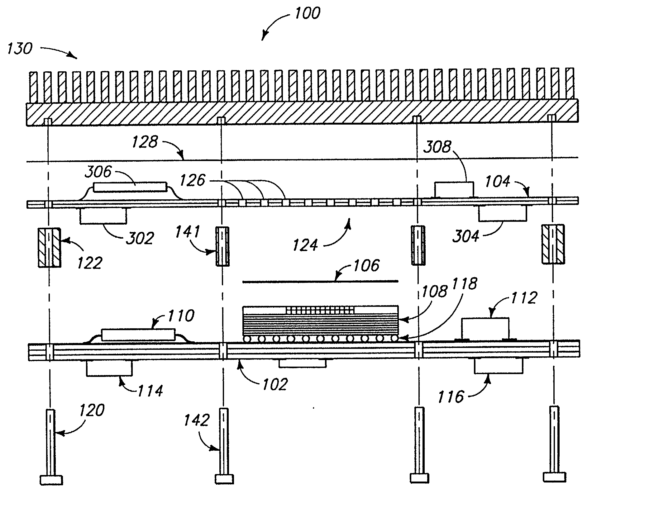
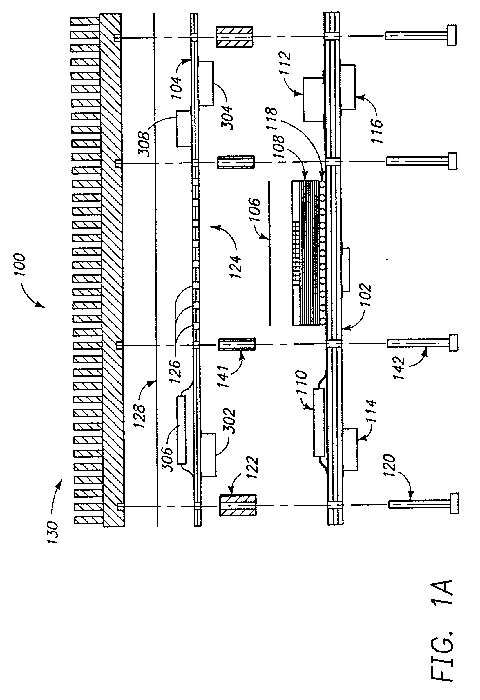
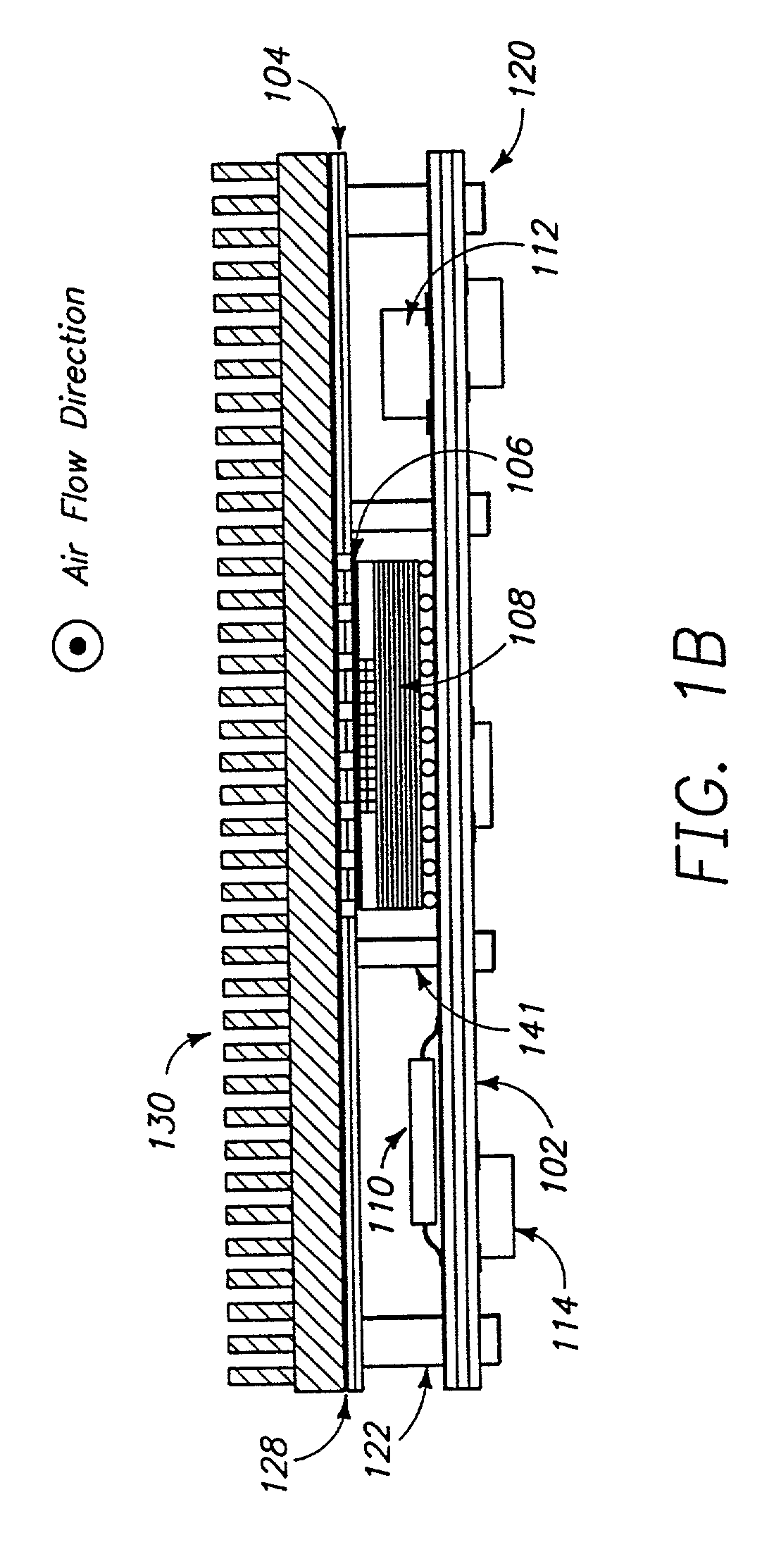
[0073] FIGS. 4A-4C illustrate the construction of a printed circuit board using the present invention. FIG. 4A illustrates an exploded view of assembly 100. Assembly 100 comprises first printed circuit board (PCB) 102, second PCB 104, and heat transfer device 106. First PCB 102 can be a single layer PCB or multi-layer PCB, where the multi-layer PCB is comprised of alternating layers of conducting and non-conducting materials to allow electrical signals to be routed from device to device on the first PCB 102. Devices 108, 114, and 116 are shown mounted on first PCB 102. Devices 114 and 116 are shown as being mounted on the opposite side of first PCB 102 as device 108. This illustrates that first PCB 102 can have devices 108, 114, and 116 mounted on both sides.

[0074] Device 108 is coupled to first PCB 102 via a Ball Grid Array (BGA) 118. BGA 118 provides electrical contacts between device 108 and first PCB 102. Other methods of electrical coupling between device 108 and first PCB 102 ...


PUM


Abstract

A modular circuit board assembly is disclosed. The modular circuit board assembly comprises a substrate, a circuit board, and a component, disposed between the circuit board and the substrate, the component physically and electrically coupled to the substrate. In one embodiment, the circuit board also comprises an aperture allowing for the transmission of thermal energy from the component to a heat sink. In still another embodiment of the invention, the heat sink includes a mesa having surface features cooperatively interacting with surface features on the component or members mounted on the component to provide for location and/or retention.

Description

[0001] This application claims benefit of the following U.S. Provisional Patent Applications, each of which are incorporated by reference herein:[0002] Application Serial No. 60 / 196,059, entitled "EMI FRAME WITH POWER FEED-THROUGHS AND THERMAL INTERFACE MATERIAL IN AN AGGREGATE DIAMOND MIXTURE," by Joseph T. DiBene II and David H. Hartke, filed Apr. 10, 2000;[0003] Application Serial No. 60 / 219,813, entitled "HIGH CURRENT MICROPROCESSOR POWER DELIVERY SYSTEMS," by Joseph T. DiBene II, filed Jul. 21, 2000;[0004] Application Serial No. 60 / 232,971, entitled "INTEGRATED POWER DISTRIBUTION AND SEMICONDUCTOR PACKAGE," by Joseph T. DiBene II and James J. Hjerpe, filed Sep. 14, 2000;[0005] Application Serial No. 60 / 251,222, entitled "INTEGRATED POWER DELIVERY WITH FLEX CIRCUIT INTERCONNECTION FOR HIGH DENSITY POWER CIRCUITS FOR INTEGRATED CIRCUITS AND SYSTEMS," by Joseph T. DiBene II and David H. Hartke, filed Dec. 4, 2000;[0006] Application Serial No. 60 / 251,223, entitled "MICRO-I-PAK FOR ...

Claims


Application Information

Patent Timeline
IPC IPC(8): G06F1/18H01L23/427H01R4/64H05K1/02H05K1/14H05K3/30H05K3/36H05K7/10H05K7/20
CPCG06F1/18H01R12/52G06F1/189H01L23/427H01L2924/15192H01L2924/3011H01R4/64H05K1/0206H05K1/0263H05K1/141H05K1/144H05K3/301H05K3/368H05K7/1092H05K2201/10318H05K2201/10325H05K2201/10598H05K2201/10704H05K2201/10734H05K2201/2018H05K2201/2036H01L2224/16225G06F1/182H01L2224/73253H01L2924/00014H01L2224/0401
Inventor DIBENE, II, JOSEPH T.HARTKE, DAVID H.
Owner INCEP TECH
Why Eureka
Try Eureka