Process for forming deep and shallow insulative regions of an integrated circuit

a technology of integrated circuits and insulative regions, which is applied in the direction of basic electric elements, electrical equipment, semiconductor devices, etc., can solve the problems of increased collector/substrat capacitance, lower integration level, and large overall size of transistors

Inactive Publication Date: 2002-02-07
STMICROELECTRONICS SRL
View PDF0 Cites 12 Cited by
  • Summary
  • Abstract
  • Description
  • Claims
  • Application Information

AI Technical Summary

Problems solved by technology

This results in an increased collector / substrate capacitance and a larger overall size of the transistor, and therefore a lower level of integration.
Rapid thermal oxidation softens the corners of the trenches, which would otherwise constitute areas of stress concentration leading to the onset of dislocations.
These cups lead to the formation of a spurious transistor at the corner of the active area, and this leads to a lack of homogeneity of the threshold voltage of the transistor in the active area, the voltage being higher at the centre than at the edge, and this increases the leakage currents of the transistor as a whole.

Method used


Image

  • Process for forming deep and shallow insulative regions of an integrated circuit
  • Process for forming deep and shallow insulative regions of an integrated circuit
  • Process for forming deep and shallow insulative regions of an integrated circuit

Examples


Embodiment Construction

[0040] However, it should be understood that these embodiments are only examples of the many advantageous uses of the innovative teachings herein. In general, statements made in the specification of the present application do not necessarily limit any of the various claimed inventions. Moreover, some statements may apply to some inventive features but not to others. In general, unless otherwise indicated, singular elements may be in the plural and vice versa with no loss of generality.

[0041] In the drawing like numerals refer to like parts through several views.

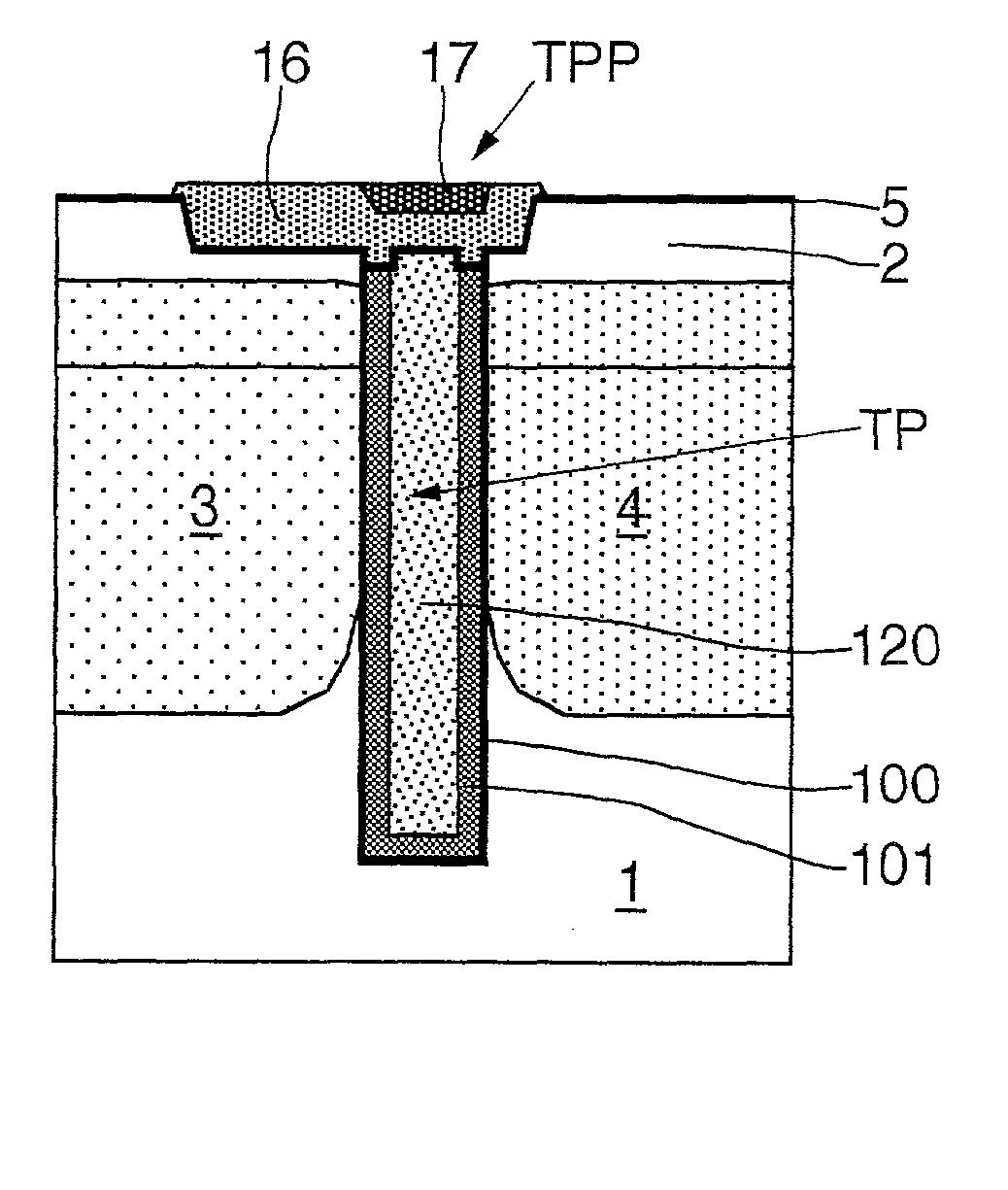
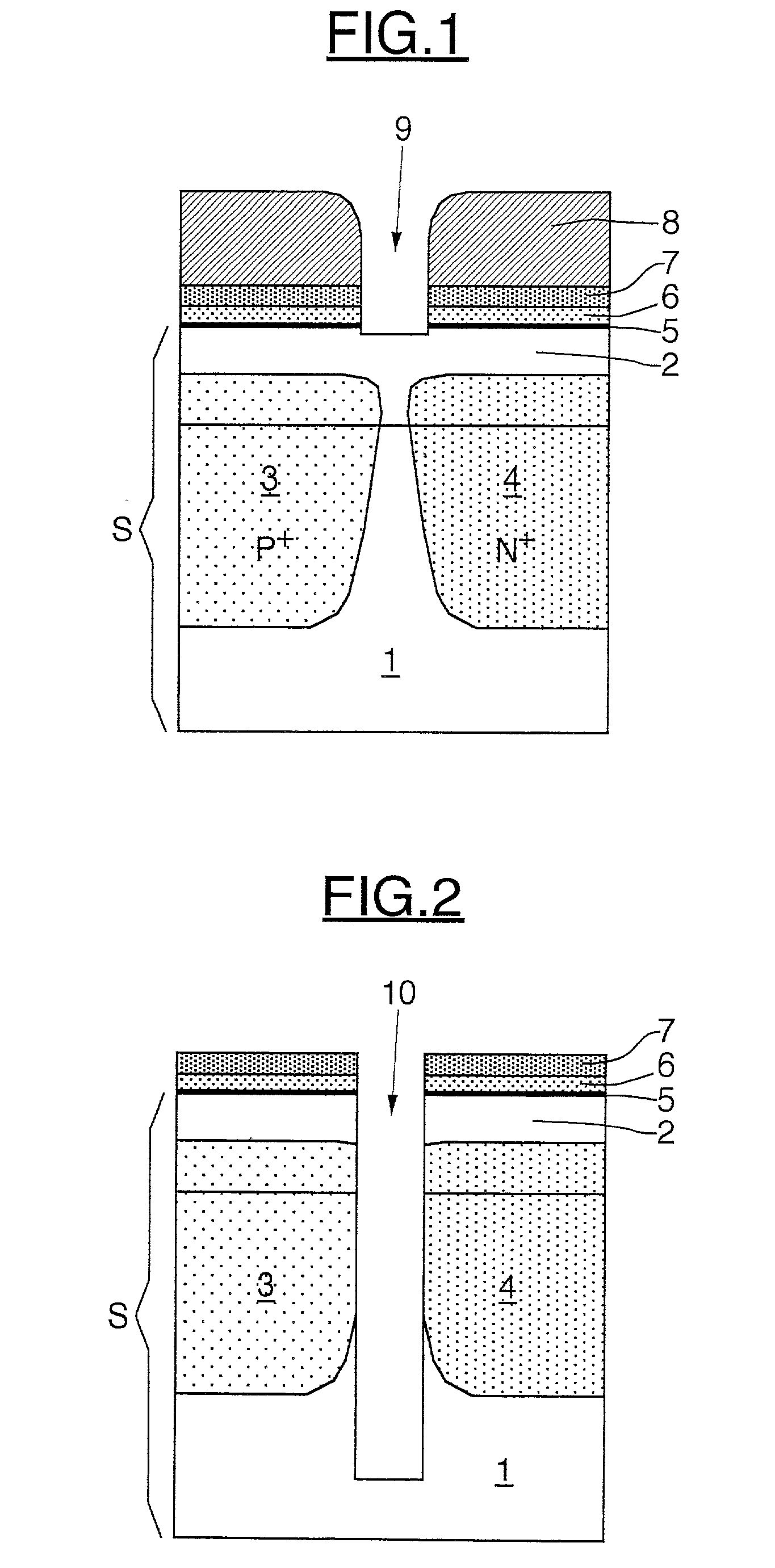
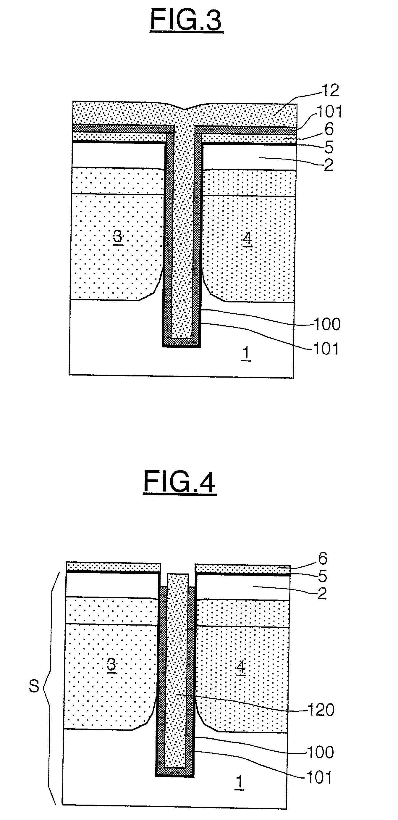
[0042] FIG. 1 shows a silicon semiconductor substrate 1, for example of the P type. P.sup.+-doped and N.sup.+-doped buried layers 3 and 4 are implanted on the silicon substrate. A layer 2 of N silicon typically 1 micron thick is then grown epitaxially.

[0043] The buried layer 4 provides a buried connecting layer between the extrinsic collector well of the bipolar transistor to be made subsequently and the intrinsic collector t...


PUM


Abstract

Prior fabricating the transistors, a phase of forming a deep insulative trench in the substrate is followed by a phase of forming a shallow insulative trench in the substrate and extending the deep trench. The phase of forming the deep trench includes coating the inside walls of the deep trench with an initial oxide layer and filling the deep trench with silicon inside an envelope formed from an insulative material. The phase of forming the shallow trench includes coating the inside walls of the shallow trench with an initial oxide layer and filling the shallow trench with an insulative material.

Description

[0001] This application is based upon and claims priority from prior French Patent Application No. 0008686, filed Jul. 4, 2000, the disclosure of which is hereby incorporated by reference in its entirety.[0002] 1. Field of the Invention[0003] The present invention generally relates to the field of integrated circuits and more particularly to forming insulative regions for electrically isolating bipolar and biCMOS transistors, especially transistors for radio frequency applications.[0004] 2. Description of Related Art[0005] Deep insulative trenches formed all around a bipolar transistor significantlyreduce the collector / substrate capacitance in radio frequency applications. The maximum frequency of oscillation of the transistors is inversely proportional to the square root of the collector / substrate capacitance.[0006] During the fabrication of MOS and bipolar transistors, deep trenches are excavated into the substrate of the integrated circuit. These deep trenches are often filled wi...

Claims


Application Information

Patent Timeline
Patent Type & Authority Applications(United States)
IPC IPC(8): H01L21/316H01L21/762H01L21/763
CPCH01L21/02238H01L21/02255H01L21/31662H01L21/76229H01L21/76232H01L21/763
Inventor MARTY, MICHELBAUDRY, HELENELEVERD, FRANCOIS
Owner STMICROELECTRONICS SRL
Why Eureka
Try Eureka