Method for fabricating different gate oxide thickness within the same chip

a technology of gate oxide and chip, which is applied in the direction of basic electric elements, electrical equipment, semiconductor devices, etc., can solve the problems of increasing the overall manufacturing cost, poor device performance, and significantly reducing the speed

Inactive Publication Date: 2003-05-22
GLOBALFOUNDRIES INC
View PDF0 Cites 12 Cited by
  • Summary
  • Abstract
  • Description
  • Claims
  • Application Information

AI Technical Summary

Benefits of technology

[0012] The present invention makes it possible to increase or extend the range of differences in thicknesses between thicker and thinner silicon dioxide layers. According to the present invention, at least two different ions are used, one being nitrogen and the other being chlorine and / or bromine. The nitrogen is used in those areas where a slower or reduced oxidation rate is desired, while chlorine and / or bromine is used in those areas where a faster oxidation rate is desired. By employing the chlorine and bromine, the dosage of the nitrogen used can be lower than that required by prior art processes. This in turn, significantly reduces, if not entirely eliminates, problems discussed above due to nitrogen doping.
[0017] Moreover, according to the present invention, when more than two oxide thicknesses are desired, more than one nitrogen and / or chlorine and / or bromine implantation step can be employed with different dosages of nitrogen and / or chlorine and / or bromine. This makes it possible to tailor and fine tune many silicon dioxide thicknesses as is desired on the substrate. Furthermore, if desired, areas of the substrate where silicon dioxide is to be formed can be left undoped to achieve one more different gate oxide thickness.

Problems solved by technology

Use of relatively thick oxide for the lower voltage transistors cause poor device performance and significantly decrease the speed.
However, such approach typically significantly increases the overall manufacturing cost and degrades the reliability as well as yield due to the potential resist residues contamination.
Besides, the oxide thickness control is more difficult because the thick oxide layer results from the combination of multiple oxide formation cycles.
However, the use of nitrogen implant alone has resulted in certain problems.
For instance, implanting nitrogen at high doses introduces beam damage in the channel region of the device.
This damage in turn results in changes in the channel impurity distributions as well as introducing silicon defects which can degrade sub-Vt leakage (off current), gate oxide breakdown voltage as well as reliability.
The problem with this process is that it depends on the dopant to enhance the oxidation rate which limits the freedom of usage because the dopant at the same time determines the substrate concentration which is a very important parameter in the device structure.
Moreover, use of fluoride ions are problematic since such are not compatible, for instance, with boron-doped PFET gates, as currently used in advanced logic CMOS.
Accordingly, using fluoride ions as discussed in U.S. Pat. No. 5,480,828 is not especially suitable for advanced CMOS from a practical application viewpoint.

Method used


Image

  • Method for fabricating different gate oxide thickness within the same chip
  • Method for fabricating different gate oxide thickness within the same chip
  • Method for fabricating different gate oxide thickness within the same chip

Examples


Embodiment Construction

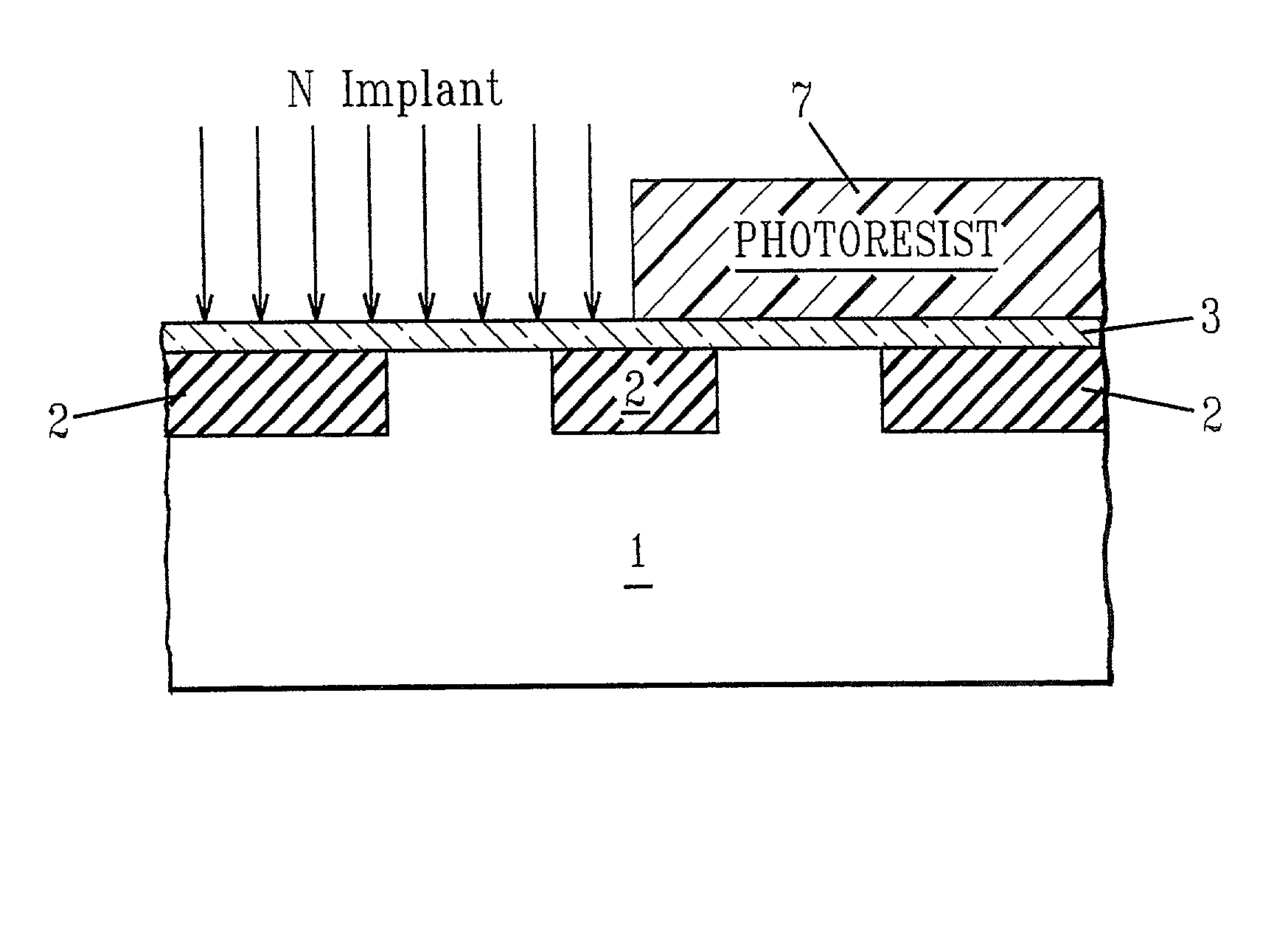
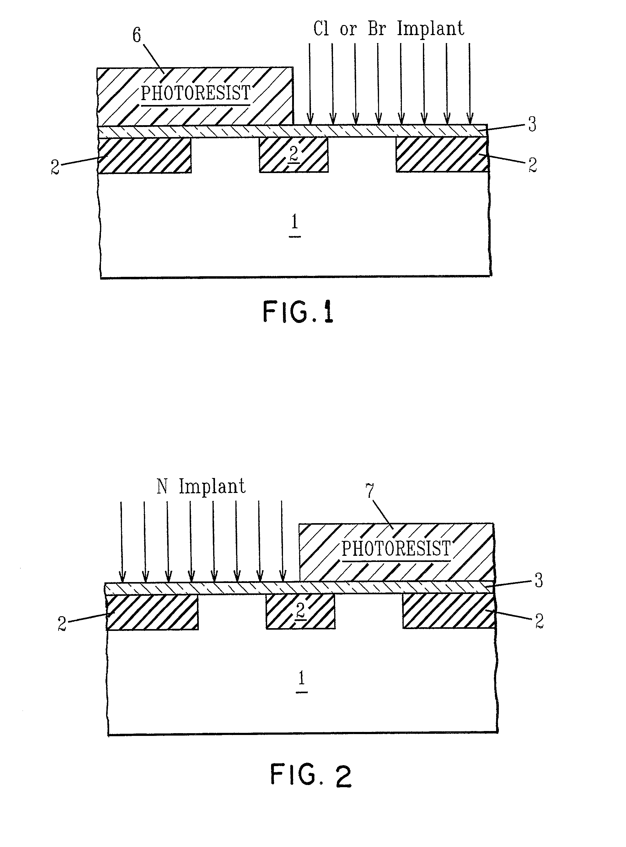
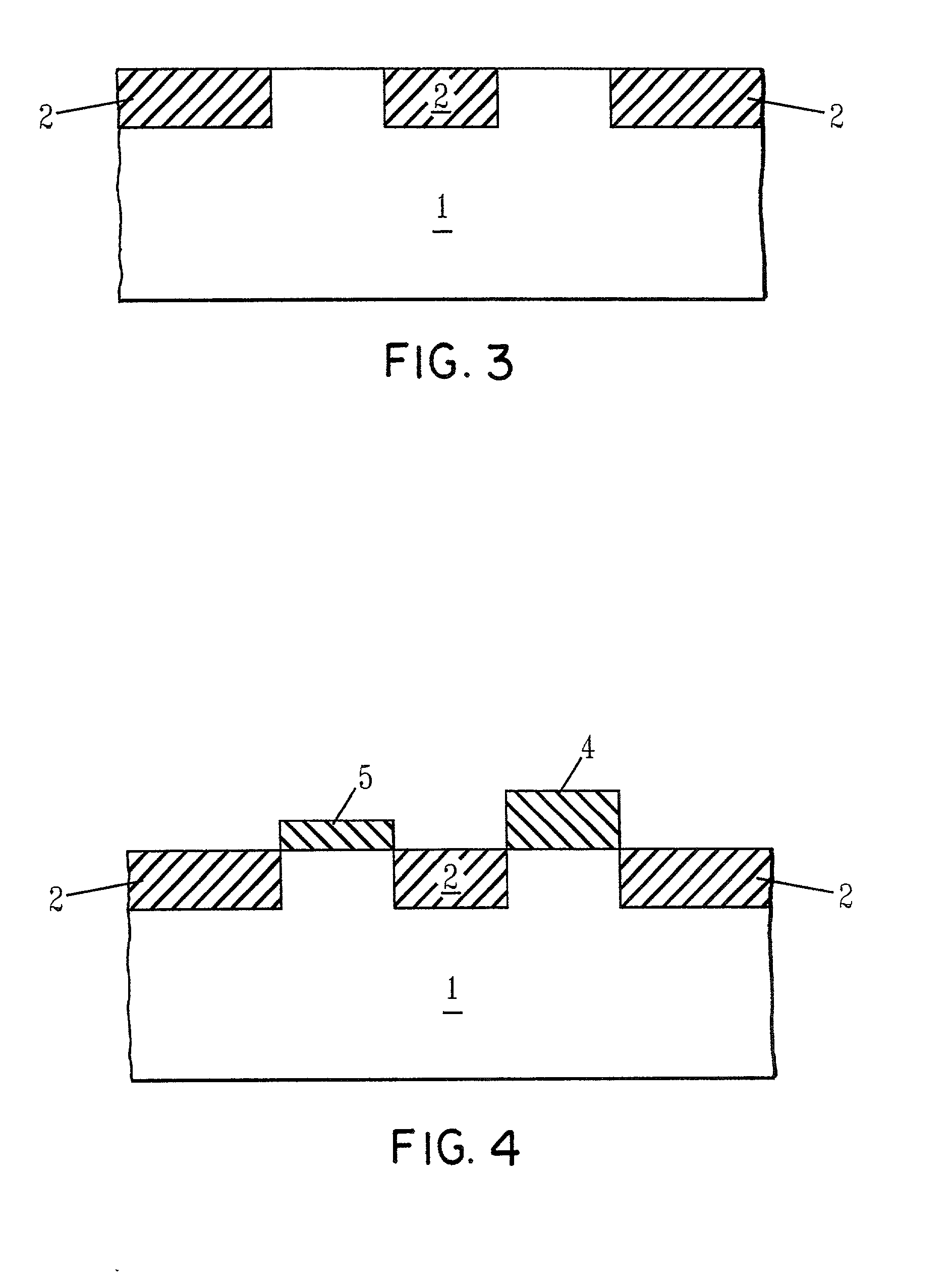
[0027] In order to facilitate an understanding of the present invention, reference is made to the figures which illustrate a portion of a partially fabricated integrated circuit. In particular, see FIG. 1 wherein is shown a semiconductor substrate 1, which is typically monocrystalline silicon or a SOI substrate (silicon on insulator). Shallow trench isolation regions 2 are formed as is conventional in the art. A layer of sacrificial silicon dioxide 3 is grown on the surface of the semiconductor substrate, typically to a thickness of about 25 to about 120 .ANG., with 60 .ANG. being an example. The sacrificial silicon dioxide layer is provided for cleaning the active silicon regions of residual nitride from the previous isolation process as well as for removing the near surface silicon which may have been damaged or contaminated in the previous processing.

[0028] By way of illustration only, the discussion that follows refers to a sequence whereby chlorine and / or bromine doping occurs ...


PUM

PropertyMeasurementUnit
energyaaaaaaaaaa
thickaaaaaaaaaa
thickaaaaaaaaaa

Abstract

A semiconductor structure having silicon dioxide layers of different thicknesses is fabricated by forming a sacrificial silicon dioxide layer on the surface of a substrate; implanting nitrogen ions through the sacrificial silicon dioxide layer into first areas of the semiconductor substrate; implanting chlorine and / or bromine ions through the sacrificial silicon dioxide layer into second areas of the semiconductor substrate where silicon dioxide having the highest thickness is to be formed; removing the sacrificial silicon dioxide layer; and then growing a layer of silicon dioxide on the surface of the semiconductor substrate. The growth rate of the silicon dioxide will be faster in the areas containing the chlorine and / or bromine ions and therefore the silicon dioxide layer will be thicker in those regions as compared to the silicon dioxide layer in the regions not containing the chlorine and / or bromine ions. The growth rate of the silicon dioxide will be slower in the areas containing the nitrogen ions and therefore the silicon dioxide layer will be thinner in those regions as compared to the silicon dioxide layer in the regions not containing the nitrogen ions. Also provided are structures obtained by the above process.

Description

[0001] The present invention is concerned with a method for simultaneously fabricating different oxide thicknesses on the same semiconductor substrate. The present invention is especially advantageous when fabricating CMOS semiconductor devices and especially for providing gate oxide insulators of different thicknesses.BACKGROUND OF INVENTION[0002] An increasing demand exists for providing semiconductor chips having gate oxide layers of varying thicknesses. In fact, the gate oxide thickness is a major concern in terms of reliability considerations when providing integrated circuit devices containing transistors and other circuit elements that operate at differing voltage levels. By way of example, a relatively thin gate oxide of about 40 .ANG. is typically grown in a conventional 1.8 volt, 0.25 micron process while a relatively thick gate oxide of about 70 .ANG. is grown in a conventional 3.3 volt, 0.5 micron process.[0003] Device scaling trends have led to low voltage operation wit...

Claims


Application Information

Patent Timeline
Patent Type & Authority Applications(United States)
IPC IPC(8): H01L21/316H01L21/8234
CPCH01L21/31662H01L21/823462Y10S148/116Y10S148/163Y10S438/981H01L21/02238
Inventor CROWDER, SCOTT W.DOMENICUCCI, ANTHONY GENEHAN, LIANG-KAIHARGROVE, MICHAEL JOHNRONSHEIM, PAUL ANDREW
Owner GLOBALFOUNDRIES INC
Why Eureka
Try Eureka