Method and apparatus for improving film deposition uniformity on a substrate

a technology of uniform film deposition and substrate, applied in the direction of coating, chemical vapor deposition coating, metallic material coating process, etc., can solve the problems of reducing the uniformity of film thickness, process completely unmanufacturable, and non-uniform film deposition rate on the surface of the wafer

Inactive Publication Date: 2002-02-21
HEY H PETER W +2
View PDF0 Cites 45 Cited by
  • Summary
  • Abstract
  • Description
  • Claims
  • Application Information

AI Technical Summary

Benefits of technology

[0022] In one embodiment of the present invention a silicide layer is selectively deposited onto silicon containing portions of a substrate. According to the selective silicide deposition process, a susceptor is first coated with a prewafer reaction layer of silicon or a silicide, and then a wafer is placed on the prewafer reaction layer coated susceptor. A deposition gas is then fed into the chamber in such a way that the deposition gas first reacts with the prewafer reaction layer on the susceptor and then reacts with the substrate. In another embodiment of the present invention a silicide layer is blanket deposited over a substrate utilizing an integrated deposition process. According to the integrated deposition process of the present invention, a wafer is placed on a susceptor and then a silicon layer is blanket deposited onto the wafer and onto the susceptor. Deposition gas then fed into the chamber where it initially reacts with the silicon on the susceptor and then reacts with silicon on the wafer. Both techniques are effective at reducing deposition "edge effects" thereby enabling uniform silicide deposition to occur.

Problems solved by technology

A problem with depositing titanium silicide by the process and apparatus described above is that the film deposition rate is non uniform across the surface of the wafer.
Edge effects substantially reduce film thickness uniformity and can make a process entirely unmanufacturable.

Method used


Image

  • Method and apparatus for improving film deposition uniformity on a substrate
  • Method and apparatus for improving film deposition uniformity on a substrate
  • Method and apparatus for improving film deposition uniformity on a substrate

Examples


Embodiment Construction

[0020] The present invention is a method and apparatus for uniformly depositing a film on a substrate. In the following description numerous specific details such as specific materials, gasses and processes have been described in order to provide a thorough understanding of the present invention. In other instances well known semiconductor equipment and manufacturing processes have not been given in detail in order to not unnecessarily obscure the present invention.

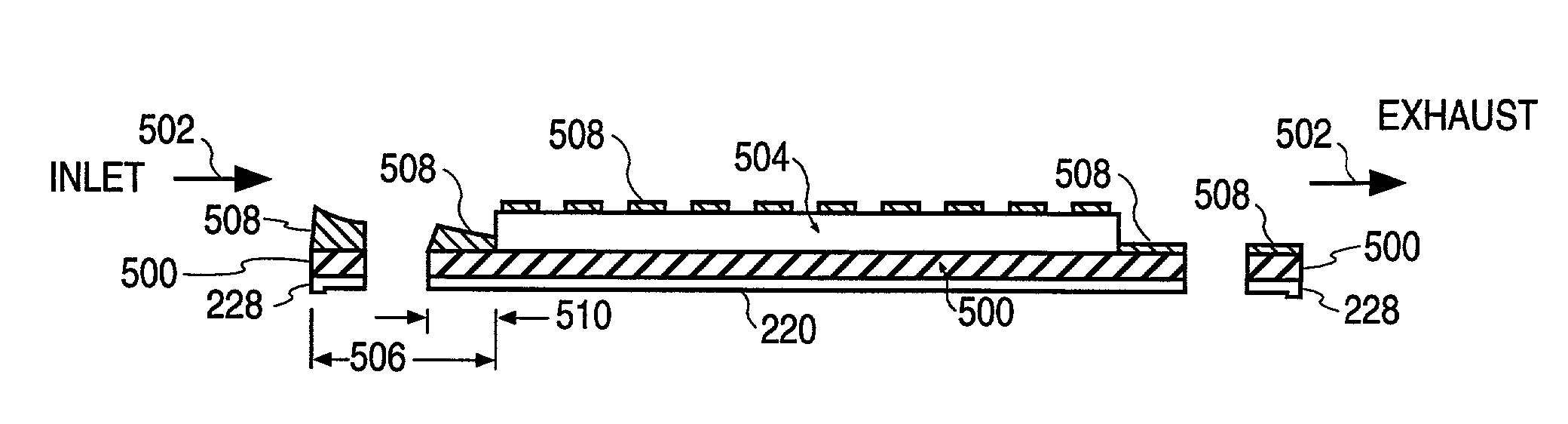
[0021] The present invention is a technique for improving the thickness uniformity of a film formed by chemical vapor deposition (CVD). According to the present invention a prewafer reaction layer is formed adjacent to a wafer prior to film deposition. The prewafer reaction layer provides an initial reaction surface for deposition gasses as they enter the reaction chamber so that initial film growth occurs on the prereaction surface as opposed to the wafer edge. By providing an initial reaction surface, the increased depo...


PUM

PropertyMeasurementUnit
pressureaaaaaaaaaa
temperatureaaaaaaaaaa
thicknessaaaaaaaaaa

Abstract

A method and apparatus for depositing a film on a substrate. According to the present invention a prewafer reaction layer is deposited onto a susceptor placed in the reaction chamber to form a prewafer reaction layer coated susceptor prior to film deposition. A deposition gas is then fed into the reaction chamber so that it flows over the prewafer reaction layer coated susceptor and the substrate to form a film on the prewafer reaction layer coated susceptor and the substrate.

Description

[0001] 1. Field of the Invention[0002] The present invention relates to the field of semiconductor manufacturing, and more specifically to a method and apparatus for uniformly depositing a thin film on a substrate.[0003] 2. Discussion of Related Art[0004] Semiconductor devices are made up of literally millions of discreet devices which are interconnected together to form functional circuits, such as microprocessors, memories and programmable logic devices. In order to improve circuit performance, the fabrication processes generally utilize low resistance metal films such as silicides to form low resistance gate electrodes, contact regions, capacitor electrodes and interconnection lines. Silicide films, such as titanium silicide, can be formed by chemical vapor deposition (CVD) processes.[0005] FIG. 1 is an illustration of a current CVD apparatus which can be used to deposit a titanium silicide film on a semiconductor wafer or substrate. A susceptor 120 divides a chamber 112 into one...

Claims


Application Information

Patent Timeline
Patent Type & Authority Applications(United States)
IPC IPC(8): C23C16/44H01L21/205H01L21/285
CPCC23C16/44C23C16/4404
Inventor HEY, H. PETER W.ACHUTHARAMAN, VEDAPURAM S.SWENBERG, JOHANES F. N.
Owner HEY H PETER W
Why Eureka
Try Eureka