Novel non-crystalline oxides for use in microelectronic, optical, and other applications

a technology of non-crystalline oxides and oxides, applied in zirconium oxides, chemistry apparatuses and processes, etc., can solve the problems of reducing the ratio of on-state current to off-state current, and volt potential drop

Inactive Publication Date: 2002-02-28
NORTH CAROLINA STATE UNIV
View PDF3 Cites 43 Cited by
  • Summary
  • Abstract
  • Description
  • Claims
  • Application Information

AI Technical Summary

Benefits of technology

0021] In another aspect, the invention provides a field effect transistor. The field effect transistor comprises an integrated circuit substrate having a first surface, source and drain regions in the substrate at the first surface in a spaced apart relationship, and a gate insulating layer on the substrate at the first surface between the spaced apart source and drain regions. The gate insulating layer comprises any of the non-crystalline oxides represented by formulas (I) or (II) described hereinbelow.

Problems solved by technology

Such a volt potential drop is potentially disadvantageous in that it begins to reduce the ratio of on- to off-state current in a field effect transistor.

Method used


Image

  • Novel non-crystalline oxides for use in microelectronic, optical, and other applications
  • Novel non-crystalline oxides for use in microelectronic, optical, and other applications

Examples


Embodiment Construction

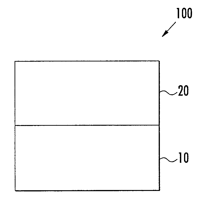
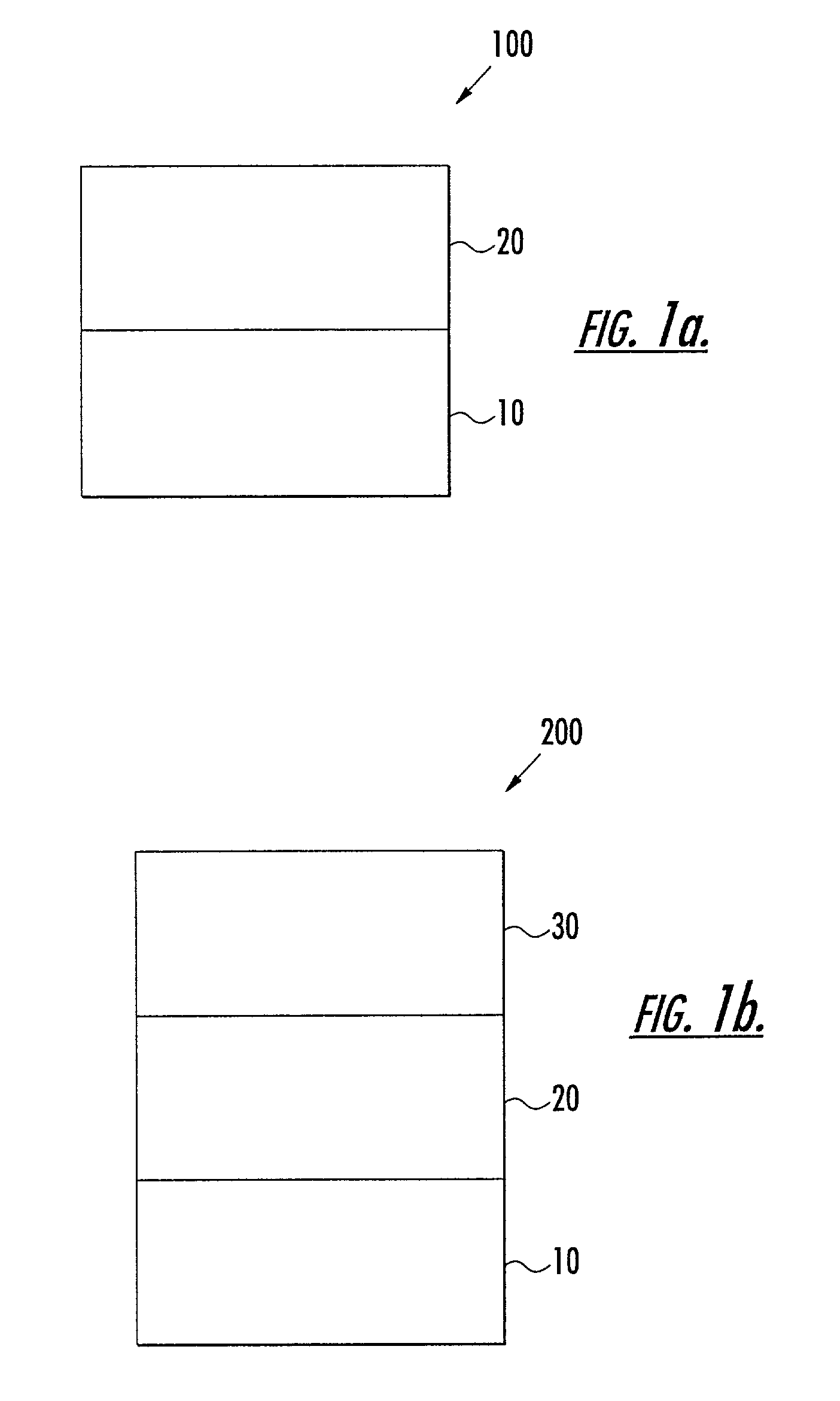
[0024] The invention will now be described in detail with reference to the following embodiments set forth herein. It should be appreciated that these embodiments merely serve to illustrate the invention and do not limit the scope of the invention. In the drawings, like numbers refer to like elements throughout. In addition, the term "on" is construed to mean a structure actually contacting an adjoining structure, or in close proximity to the adjoining structure without actually contacting it.

[0025] In one aspect, the invention provides a non-crystalline oxide represented by the formula (I):

--(ABO.sub.4).sub.x(M.sub.nO.sub.m).sub.1-x-- (I)

[0026] wherein:

[0027] A is an element selected from Group IIIA of the periodic table;

[0028] B is an element selected from Group VB of the periodic table;

[0029] O is oxygen;

[0030] M is an element selected from either Group IIIB or Group IVB of the periodic table; and n ranges from about 0.5 to about 2.5, m ranges from about 1.5 to about 3.5, and x i...


PUM

PropertyMeasurementUnit
thicknessaaaaaaaaaa
thicknessaaaaaaaaaa
gate lengthsaaaaaaaaaa

Abstract

The invention relates to non-crystalline oxides of formulas (I) and (II), and methods of forming the same, along with field effect transistors, articles of manufacture, and microelectronic devices comprising the non-crystalline oxides.

Description

[0001] The present application claims priority to U.S. Provisional Application No. 60 / 214,285 filed Jun. 26, 2001, the disclosure of which is incorporated herein by reference in its entirety.[0002] The invention generally relates to oxide-containing materials, along with articles of manufacture comprising the same, and methods of forming the same.[0003] As device dimensions are scaled according to the 1999 Technology Roadmap for Semiconductors, 1999 Edition (http: / / public.itrs.net), the equivalent gate oxide thickness, EOT, should decrease below about 1.5 nm. At this silicon dioxide (SiO.sub.2) thickness, the direct tunneling current for a one volt potential drop across the oxide is typically greater than 1 A / cm.sup.-2. Such a volt potential drop is potentially disadvantageous in that it begins to reduce the ratio of on- to off-state current in a field effect transistor. In order to attempt to reduce the off-state leakage currents due to tunneling through SiO.sub.2 and maintain a ca...

Claims


Application Information

Patent Timeline
Patent Type & Authority Applications(United States)
IPC IPC(8): C01F17/00C01B13/14C01G25/02C01G27/02C01G35/00C23C16/40H01L21/314H01L21/316H01L29/51H01L29/78H01L33/00H01L33/04H01L33/16H01L33/30H01L33/34
CPCC23C16/40H01L21/31604H01L21/31691H01L29/513H01L29/517H01L29/518H01L21/02274H01L21/02194
Inventor LUCOVSKY, GERALDPARSONS, GREGORY N.
Owner NORTH CAROLINA STATE UNIV
Why Eureka
Try Eureka