

Multilayer structure, method for manufacturing same, semiconductor device, and crystalline film
a multi-layer structure and manufacturing method technology, applied in the direction of semiconductor devices, basic electric elements, electrical appliances, etc., can solve the problems of difficult use of semiconductor devices, poor crystallinity, and insufficient semiconductor properties including conductivity, and achieve excellent crystallinity, good mobility, and excellent crystallinity. excellent
- Summary
- Abstract
- Description
- Claims
- Application Information
AI Technical Summary
Benefits of technology
Problems solved by technology
Method used
Image

Examples
example 1
1. Film Formation Apparatus
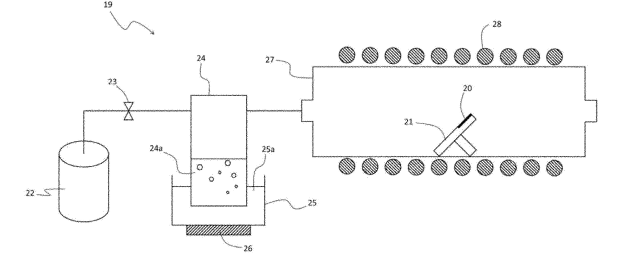
[0136]With reference to FIG. 18, a mist CVD apparatus 19 used in the working Examples is described. The mist CVD apparatus 19 was provided with a susceptor 21 to place a substrate 20, carrier gas supply means 22 to supply a carrier gas, a flow regulating valve 23 to regulate a flow rate of the carrier gas discharged from the carrier gas supply means 22, a mist generator 24 to store a raw-material solution 24a, water 25a, an ultrasonic vibration transducer 26 mounted at a bottom of the container 25, a supply pipe 27 of a quartz pipe with an inner diameter of 40 mm, and a heater 28 placed surrounding the supply pipe 27. The susceptor 21 was made from quartz and had a surface to place the substrate 20 inclined from the horizontal plane. Both the supply pipe 27 and the susceptor 21 made from quartz inhibit mixing of impurities derived from the apparatus into the film formed on the substrate 20.
[0137]As the susceptor 21, the susceptor 51 illustrated in FIGS. 19...
example 2
[0144]A multilayer structure was obtained in the same manner as in Example 1 ther than using a c-plane sapphire substrate with an off angle of 0.6° as the crystal substrate.
[0145]The crystalline film thus obtained was clean crystal without cloudiness. A phase of the crystalline film thus obtained was identified in the same manner as in Example 1 to find out that the film thus obtained was α-Ga2O3. The Hall effect was measured in the same manner as in Example lto find out that the mobility was 2 (cm2 / V·s).
example 3
[0146]A multilayer structure was obtained in the same manner as in Example 1 other than using a c-plane sapphire substrate with an off angle of 1° as the crystal substrate and changing the film formation temperature to 600° C.
[0147]The crystalline film thus obtained was clean crystal without cloudiness. A phase of the crystalline film thus obtained was identified in the same manner as in Example lto find out that the film thus obtained was α-Ga2O3. The Hall effect was measured in the same manner as in Example 1 to find out that the mobility was 2 (cm2 / V·s).
PUM
| Property | Measurement | Unit |
|---|---|---|
| off angle | aaaaa | aaaaa |
| off angle | aaaaa | aaaaa |
| thickness | aaaaa | aaaaa |
Abstract
Description
Claims
Application Information