Structure and method for controlling band offset and alignment at a crystalline oxide-on-semiconductor interface

a technology of crystalline oxide and crystalline oxide, applied in the direction of crystal growth process, transportation and packaging, natural mineral layered products, etc., can solve the problem of little attention to the electrical behavior characteristics of electronic devices whose cos structures are embodied

Inactive Publication Date: 2003-11-25
UT BATTELLE LLC
View PDF3 Cites 12 Cited by
  • Summary
  • Abstract
  • Description
  • Claims
  • Application Information

AI Technical Summary

Problems solved by technology

While perfecting techniques to construct crystalline oxide-on-semiconductor (COS) structures, however, little attention has been given to the electrical behavioral characteristics of electronic devices within which such COS structures are embodied.

Method used


Image

  • Structure and method for controlling band offset and alignment at a crystalline oxide-on-semiconductor interface
  • Structure and method for controlling band offset and alignment at a crystalline oxide-on-semiconductor interface
  • Structure and method for controlling band offset and alignment at a crystalline oxide-on-semiconductor interface

Examples


Embodiment Construction

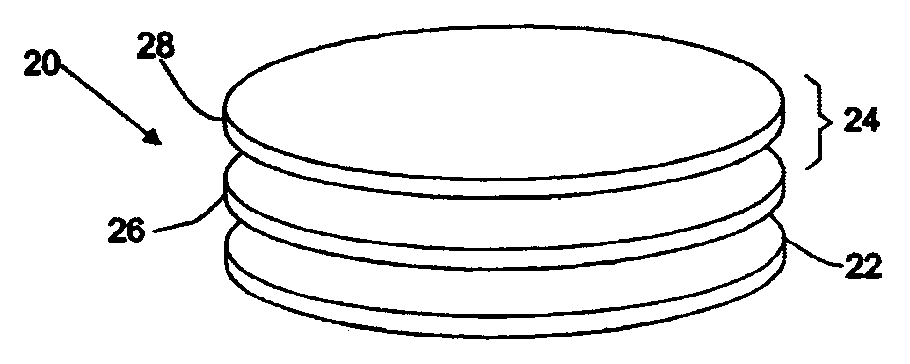
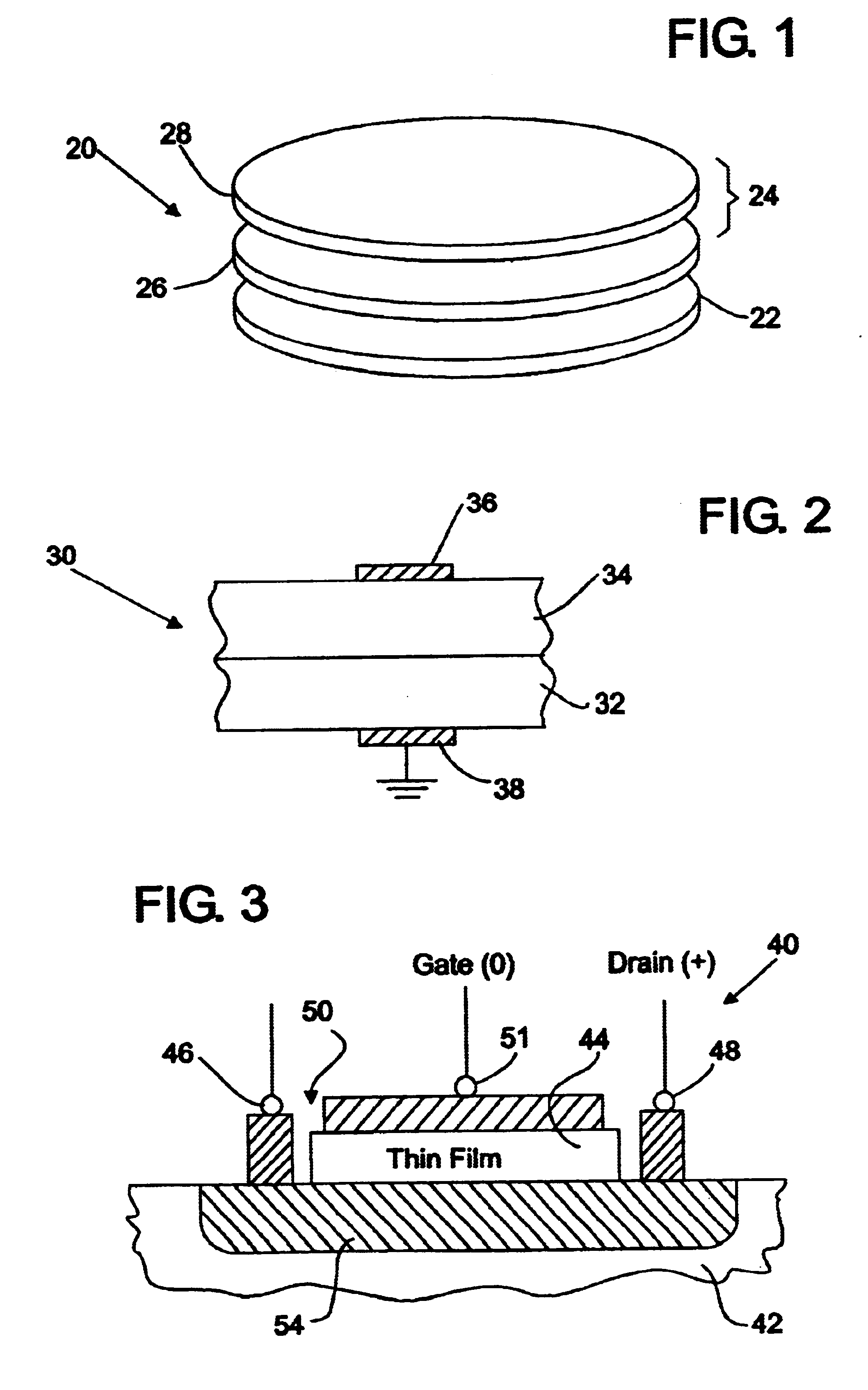
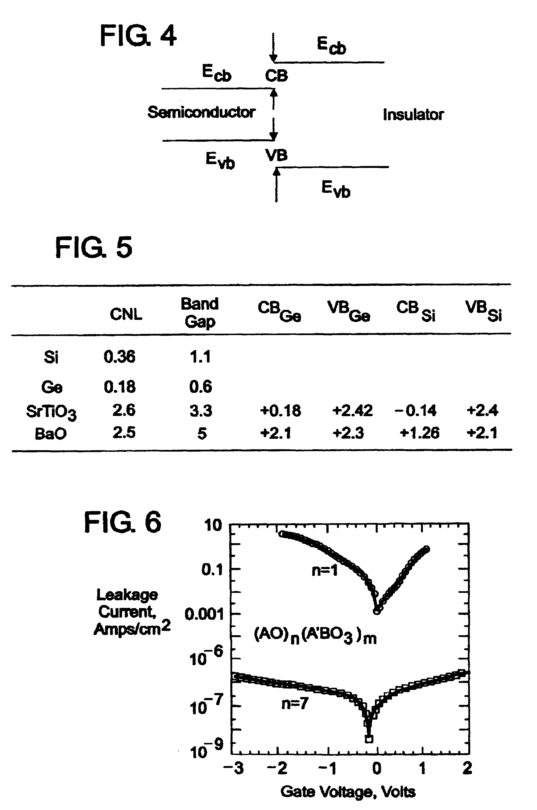
We have described in our previous patents, such as U.S. Pat. No. 5,830,270, our general series of crystalline oxide-on-semiconductor series (COS) as being designated by the general formula (AO).sub.n (A'BO.sub.3).sub.m. Within this general formula, the terms n and m are non-negative integer repeats of single layers of the oxide AO or the oxide A'BO.sub.3 which are constructed upon a semiconductor-based substrate, such as the Group IVA semiconductors silicon, germanium or a silicon-germanium alloy. Whereas each layer of the oxide AO in such a structure is planar in nature in that it has a height, or thickness, which is about equal to the height of a single AO plane, each layer of the oxide A'BO.sub.3 has a height, or thickness, which is about equal to the height of one unit cell of the A'BO.sub.3 oxide.

Moreover, the element O in the general formula represents oxygen, while the element A (or A') can be a material found in Group IA, IIA or IVB of the periodic table of elements and the ...


PUM

PropertyMeasurementUnit
gate voltageaaaaaaaaaa
temperatureaaaaaaaaaa

Abstract

A crystalline oxide-on-semiconductor structure and a process for constructing the structure involves a substrate of silicon, germanium or a silicon-germanium alloy and an epitaxial thin film overlying the surface of the substrate wherein the thin film consists of a first epitaxial stratum of single atomic plane layers of an alkaline earth oxide designated generally as (AO)n and a second stratum of single unit cell layers of an oxide material designated as (A'BO3)m so that the multilayer film arranged upon the substrate surface is designated (AO)n(A'BO3)m wherein n is an integer repeat of single atomic plane layers of the alkaline earth oxide AO and m is an integer repeat of single unit cell layers of the A'BO3 oxide material. Within the multilayer film, the values of n and m have been selected to provide the structure with a desired electrical structure at the substrate / thin film interface that can be optimized to control band offset and alignment.

Description

This invention relates to the structure of electronic devices, such as capacitors and transistors, embodying a thin film which has been grown upon a semiconductor substrate and more particularly is concerned with the electrical characteristics of such structures when embodied in electronic devices.We have described in our prior U.S. patents, such as U.S. Pat. No. 5,830,270, various processes for constructing thin films upon a semiconductor substrate with few, if any, dislocations or other undesirable defects at the thin-film / substrate interface. Some of our construction processes involve a layer-by-layer build up of an epitaxial, and sometimes commensurate, oxide upon the substrate (i.e., a crystalline oxide-on-semiconductor substrate, or COS, structure) wherein each layer in the build up process is comprised of a constituent plane of the oxide. For example, in our U.S. Pat. No. 5,830,270, we describe a build-up of a perovskite oxide upon a substrate as having the general formula (A...

Claims


Application Information

Patent Timeline
Patent Type & Authority Patents(United States)
IPC IPC(8): C30B25/02C30B23/02H01L21/28H01L29/49H01L21/02H01L29/40
CPCC30B23/02H01L21/28291H01L29/4983C30B25/02C30B29/32C30B29/16Y10T428/12611Y10T428/12618Y10T428/12528C30B23/002H01L29/40111
Inventor MCKEE, RODNEY A.WALKER, FREDERICK J.
Owner UT BATTELLE LLC
Why Eureka
Try Eureka