
Semiconductor device

a technology of semiconductors and devices, applied in the direction of semiconductor devices, basic electric elements, electrical equipment, etc., can solve the problems of impairing semiconductor properties and increasing manufacturing costs, and achieve excellent semiconductor properties and schottky characteristics

Active Publication Date: 2017-06-22
FLOSFIA
View PDF2 Cites 14 Cited by
  • Summary
  • Abstract
  • Description
  • Claims
  • Application Information

AI Technical Summary

Benefits of technology

The semiconductor device in this patent has good properties and works well with Schottky.

Problems solved by technology

However, having a β-gallic structure, β-Ga2O3 is not always preferred to be used in semiconductor devices, different from crystal systems generally used in electronic materials and the like.
Growth of a β-Ga2O3 thin film requires a high substrate temperature and a high degree of vacuum, causing a problem of an increase in manufacturing costs.
Unfortunately, application of the electrodes in PTLs 1 to 3 to a semiconductor device that uses α-Ga2O3 as a semiconductor causes a problem, such as not functioning as a Schottky electrode or an ohmic electrode, failing to attach the electrode to the film, and impairing semiconductor properties.

Method used


Image

  • Semiconductor device
  • Semiconductor device
  • Semiconductor device

Examples


example 1

[0107]1. Formation of n+type Semiconductor Layer

[0108]1-1. Film Formation Apparatus

[0109]With reference to FIG. 5, a mist CVD apparatus 1 used in the present Example is described. The mist CVD apparatus 1 included a carrier gas source 2a to supply a carrier gas, a flow regulating valve 3a to regulate a flow rate of the carrier gas discharged from the carrier gas source 2a, a dilution carrier gas source 2b to supply a dilution carrier gas, a flow regulating valve 3b to regulate the flow rate of the dilution carrier gas discharged from the dilution carrier gas source 2b, a mist generator 4 to store a raw-material solution 4a, a container 5 to keep water 5a, an ultrasonic vibration transducer 6 mounted at a bottom of the container 5, a film formation chamber 7, a supply pipe 9 connecting the mist generator 4 to the film formation chamber 7, a hot plate 8 placed in the film formation chamber 7, and an exhaust outlet 11 to exhaust the mist, the droplets, and the exhaust gas after thermal...

example 2

[0135]A semiconductor device was obtained in the same manner as Example 1 other than changing, during formation of the n+type semiconductor layer, the film formation temperature to 525° C. and the film formation time to 20 minutes. The n+type semiconductor layer had a thickness of 0.5 μm. The semiconductor device thus obtained was subjected to IV measurement. Results are illustrated in FIG. 8. The on resistance (differential resistance) was checked to be found as 0.11 mΩ cm2.

example 3

[0136]A semiconductor device was obtained in the same manner as Example 1 other than (1) containing, during formation of the n-type semiconductor layer, deuterium bromide acid at a volume ratio of 15% in the raw-material solution and changing the film formation time to 8 hours, (2) changing, during formation of the n+type semiconductor layer, the film formation temperature to 500° C. and the film formation time to 110 minutes, and (3) laminating, during formation of the first metal layer (Schottky electrode), a Ti layer and an Au layer on the n-type semiconductor layer respectively by electron beam evaporation. The semiconductor device thus obtained was subjected to IV measurement. Results are illustrated in FIG. 9. As clearly seen from FIG. 9, it is found that good semiconductor properties and Schottky characteristics are exhibited.


PUM


Abstract

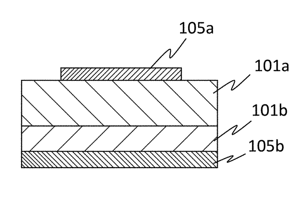
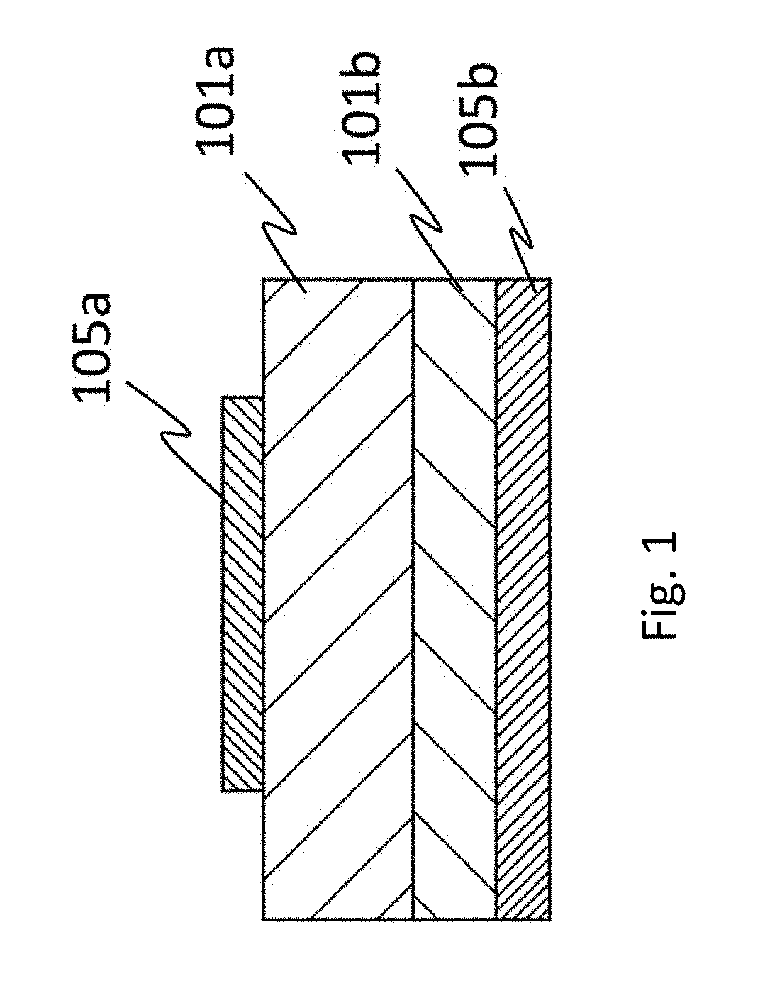
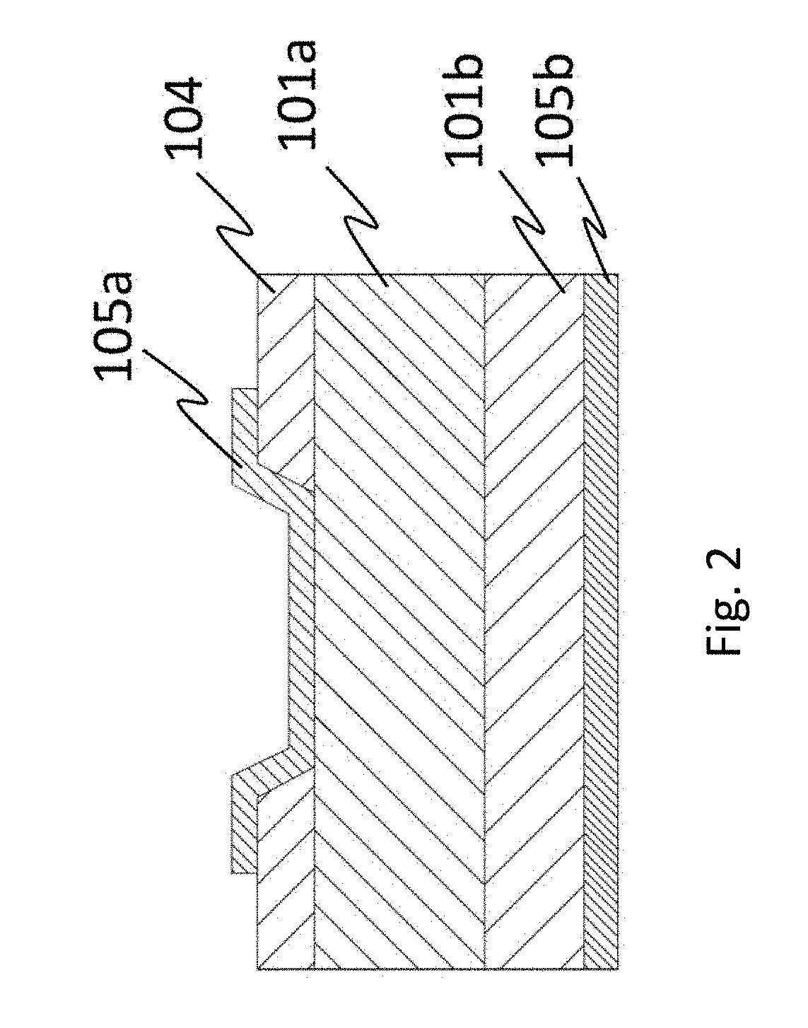
A semiconductor device is provided that is excellent in semiconductor properties and Schottky characteristics. A semiconductor device includes: a semiconductor layer containing a crystalline oxide semiconductor with a corundum structure as a major component; and a Schottky electrode on the semiconductor layer, wherein the Schottky electrode is formed by containing a metal of Groups 4-9 of the periodic table, thereby manufacturing a semiconductor device excellent in semiconductor properties and Schottky characteristics without impairing the semiconductor properties to use the semiconductor device thus obtained for a power device and the like.

Description

TECHNICAL FIELD[0001]The present invention relates to a semiconductor device particularly useful for a power device.BACKGROUND ART[0002]Gallium oxide (Ga2O3) is a transparent semiconductor that has a band gap as wide as 4.8-5.3 eV at room temperature and absorbs almost no visible light and ultraviolet light. It is accordingly a promising material for use in optical and electronic devices and transparent electronics operated particularly in a deep ultraviolet region. In recent years, photodetectors, light emitting diodes (LED), and transistors based on gallium oxide (Ga2O3) have been developed (refer to NPL 1).[0003]Gallium oxide (Ga2O3) has five crystal structures of α, β, γ, δ, and ∈, and generally the most stable structure is β-Ga2O3. However, having a β-gallic structure, β-Ga2O3 is not always preferred to be used in semiconductor devices, different from crystal systems generally used in electronic materials and the like. Growth of a β-Ga2O3 thin film requires a high substrate tem...

Claims


Application Information

Patent Timeline
IPC IPC(8): H01L29/47H01L29/41
CPCH01L29/41H01L29/47H01L29/24H01L29/872H01L29/66969H01L29/04H01L21/02414H01L21/0242H01L21/02565H01L21/02576H01L21/02581H01L21/02628H01L29/435H01L29/66143H01L29/43
Inventor ODA, MASAYATOKUDA, RIEKAMBARA, HITOSHIKAWARA, KATSUAKIHITORA, TOSHIMI
Owner FLOSFIA
Learn More