

Programmable impedance control circuit
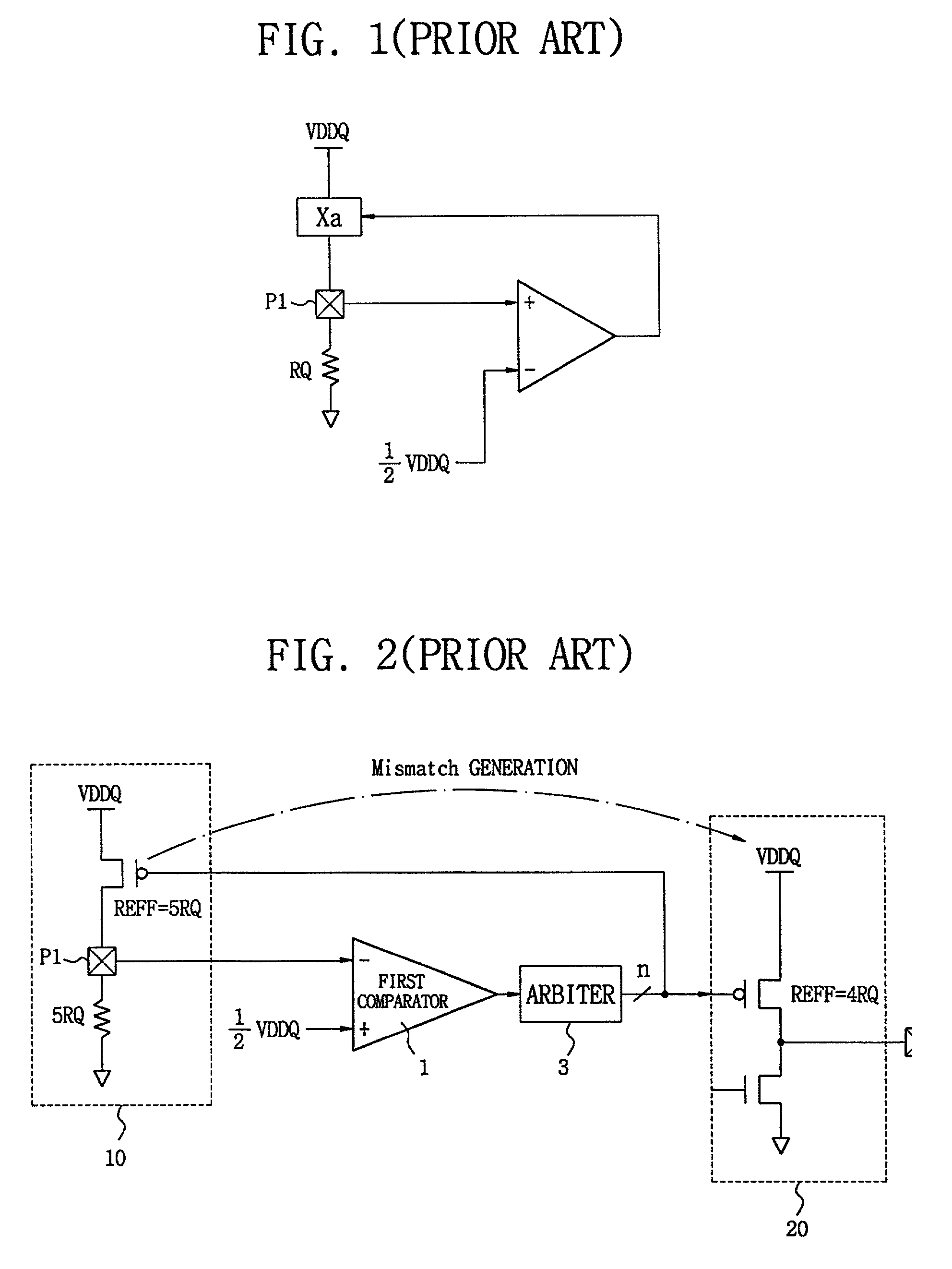
a control circuit and impedance technology, applied in logic circuit coupling/interface arrangement, pulse technique, instruments, etc., can solve the problems of mismatch errors in the measurement of external impedance by the controller, increase the consumption of power, and difficulty in properly terminating with matching impedance with fixed resistan
- Summary
- Abstract
- Description
- Claims
- Application Information
AI Technical Summary
Problems solved by technology
Method used
Image

Examples
first embodiment
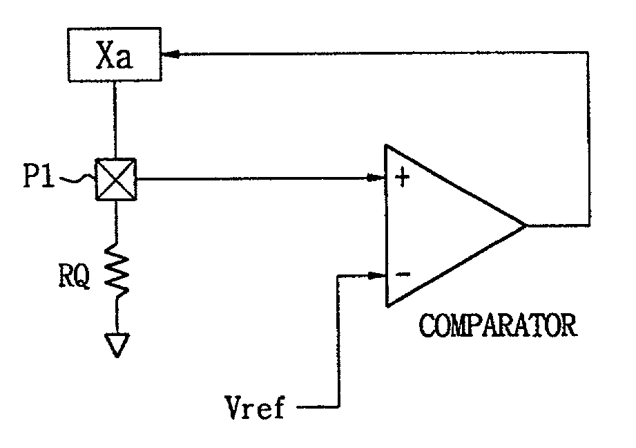
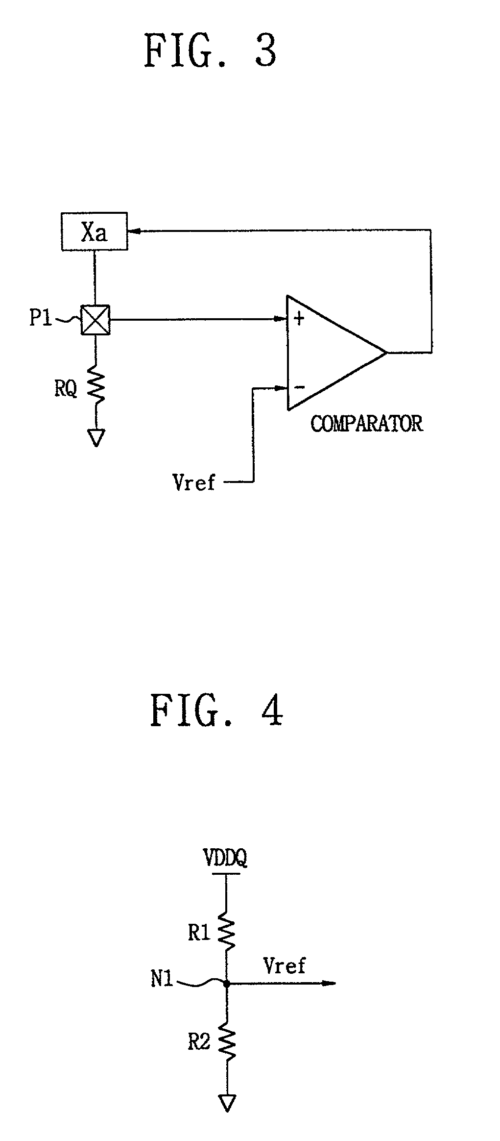
[0060] Referring to FIG. 7, there is shown a schematic of a programmable impedance control circuit in which an optional reference voltage is employed according to the present invention. The circuit comprises a pull-up circuit comprising a first MOS array 101 connected to VDDQ, a first pad P1, an external resistance 102 RQ, a low-pass filter LPF 103, a reference voltage generator 130, a first detector 120, a first latch 151, a first data output buffer 153, an off-chip up-driver OCD UP_DRIVER, and an up-terminator 159.
[0061] Also provided is a pull-down circuit comprising a second MOS array 107, a third MOS array 109, a second detector 140, a second latch 155, a second data output buffer 157, an off-chip down-driver OCD DOWN-DRIVER and a down-terminator 161.
[0062] The circuit uses M times internal impedance (N.noteq.M) in accordance with N times the external impedance RQ attached to the system by the user. Its operation is as follows:
[0063] First, the first MOS array 101 in the pull-u...
second embodiment
[0068] Next, the operation of the programmable impedance control circuit for generating an optional reference voltage by an analog method according to the present invention is explained in detail with reference to FIG. 8.
[0069] FIG. 8 is a schematic of another embodiment of the invention. In this circuit, when a current source is used as a detecting circuit and a reference voltage is adopted as (5 / 8)VDDQ, the flowing current is the same as when the VDDQ / 2 voltage is connected to a .times.4 external resistance. A current source PMOS 1 is supplied with VDDQ or VDD voltage. The circuit does not become responsive to noises in the pad P1 because of the PMOS 1. The external resistance RQ has an N times the external impedance. The pad P1 outputs the voltage obtained in combination of the PMOS 1 and the external resistance RQ. The first reference voltage generator 210 generates the reference voltage corresponding to N / (N+M) times VDDQ. The first comparator 223 compares the output voltage fr...
PUM
 Abstract
Description
Claims
Application Information