
Circuit for linearizing electronic devices

a technology of linearizing electronic devices and circuits, applied in amplifier modifications to reduce non-linear distortion, gain control, high frequency amplifiers, etc., can solve the problems of reducing the sensitivity of receivers, and affecting the quality of desired signals

Inactive Publication Date: 2002-06-06
QUALCOMM INC
View PDF8 Cites 21 Cited by
  • Summary
  • Abstract
  • Description
  • Claims
  • Application Information

AI Technical Summary

Problems solved by technology

Unfortunately, when the RF amplifiers and mixers handle desired received signals in a presence of strong interferers, distortion often results from the strong interferers that can degrade the quality of the desired signal.
The distortion products that fall in the band of the received signal are most dangerous.
If one of these signals falls in band of the desired signal, it may degrade receiver sensitivity.
Conventionally, it is difficult to achieve low levels of the distortion inasmuch as the third degree nonlinearity of the circuit is an inherent property of amplifying active devices.
Typically, a lower distortion is achieved at the expense of an increased DC current consumption.
The latter is undesirable especially in a wireless communication system powered by a battery where the higher current consumption results in a shorter battery life and, thus, a shorter system operation (for example, the talk time of the cellular phones).
Thus, the choke doesn't prevent the buffer from forcing the transistor input voltage to follow the common terminal voltage at the mentioned frequencies.

Method used


Image

  • Circuit for linearizing electronic devices
  • Circuit for linearizing electronic devices
  • Circuit for linearizing electronic devices

Examples


Embodiment Construction

[0024] Illustrative embodiments and exemplary applications will now be described with reference to the accompanying drawings to disclose the advantageous teachings of the present invention.

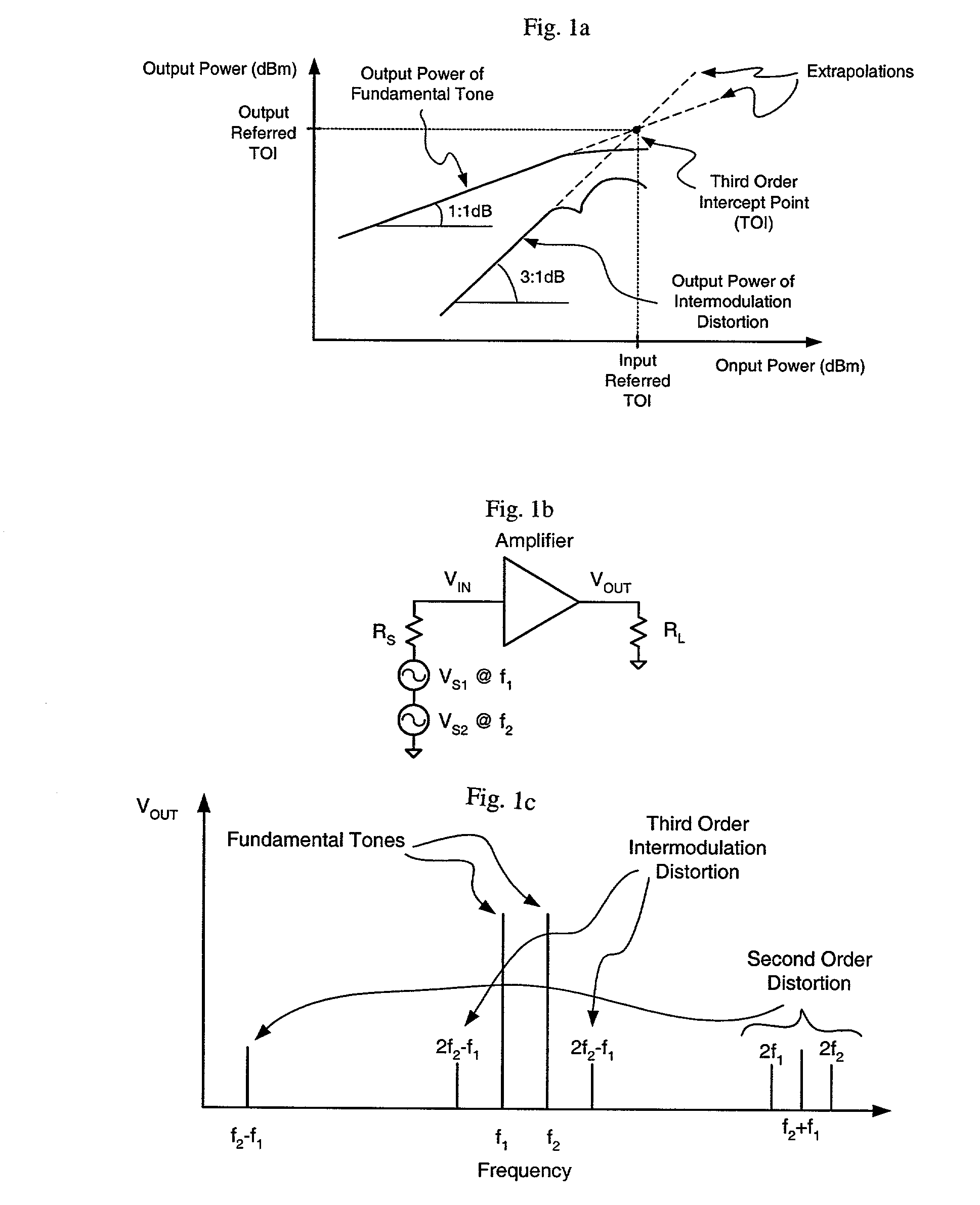
[0025] The level of the third-order intermodulation (IM3) distortion product generated by a nonlinear circuit at small input power levels is usually estimated from a third-order intercept point (TOIP) measured with a two-tone input signal. This is illustrated in FIGS. 1a and 1b.

[0026] FIG. 1a is a graph of output power verses input power for a typical RF amplifier showing the third order intercept point between the extrapolated output power associated with fundamental tones and the extrapolated output power associated with intermodulation distortion resulting therefrom. When the two fundamental tones (f.sub.1 and f.sub.2) representing two interferers are applied to a transistor, its nonlinear characteristics generate spurious responses in the output voltage. This is depicted in FIG. 1b.

[0027] FIG....


PUM


Abstract

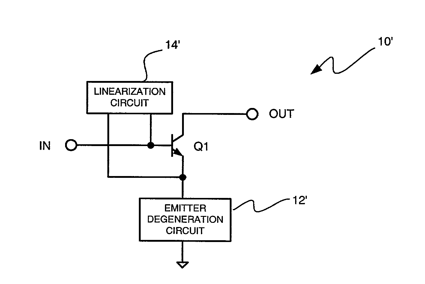
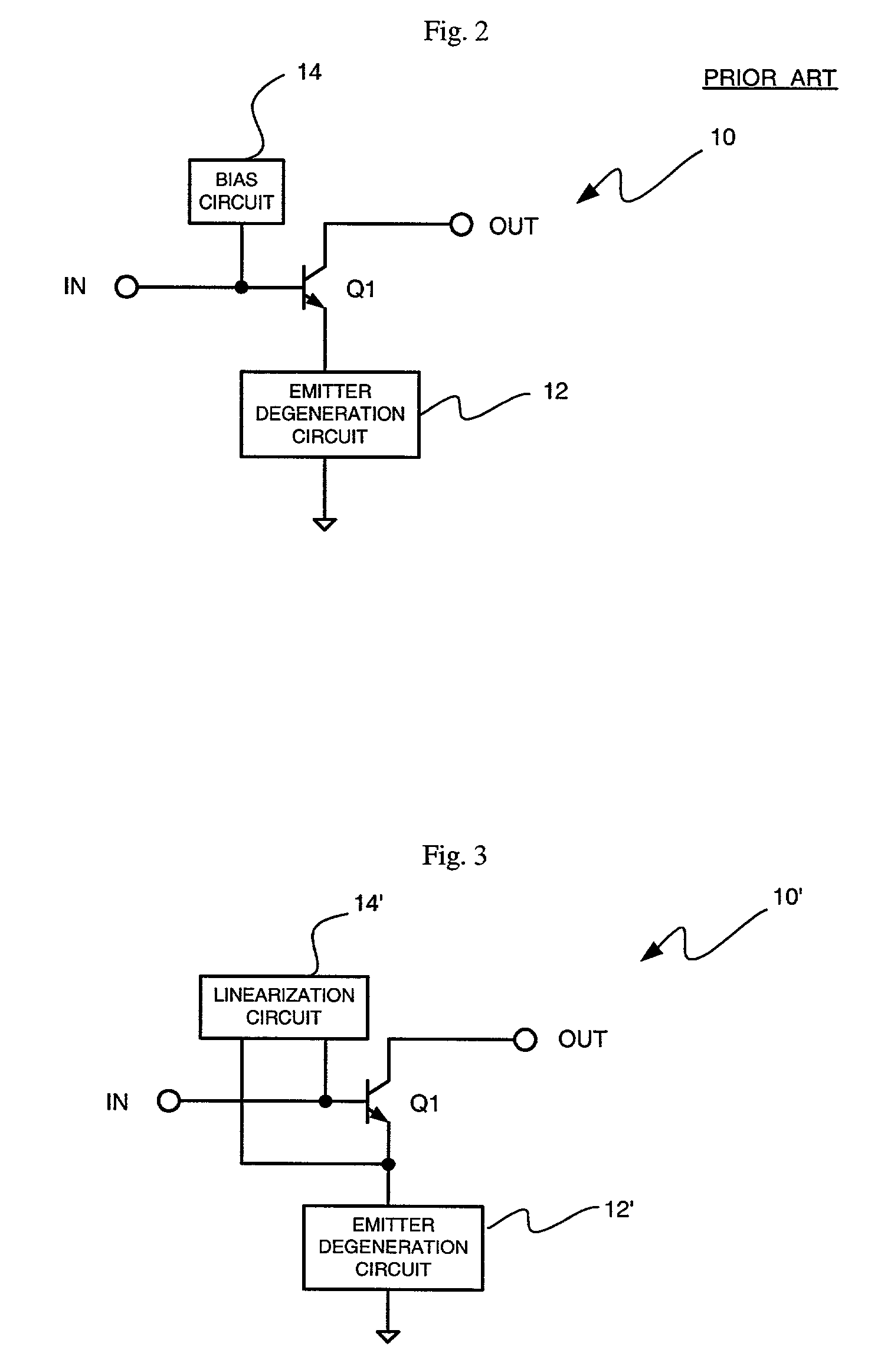
A radio frequency amplifier with improved linearity and minimal third-order distortion. The amplifier includes a first transistor having first, second and third terminals with the first terminal being an input terminal and the second terminal being the output terminal and the third terminal being a common terminal. A linearization circuit is included having first and second terminals. The first terminal is connected to the common terminal of the transistor and the second terminal is connected to the input terminal of the transistor. In a specific embodiment, the linearization circuit is implemented as a unity gain buffer with an input terminal connected to the common terminal of the transistor and an output terminal connected to the input terminal of the transistor. In accordance with the inventive teachings, the buffer has a low gain and high output impedance at first frequency (f1) of a first signal applied to the circuit and a second frequency (f2) of a second signal applied to the circuit and a unity gain and low output impedance a difference between the first and second frequencies. In another specific embodiment, the inductor is inserted between the output of the unity gain buffer and the input terminal of the transistor. In alternative embodiments, circuitry is shown for providing a direct current offset at the input of the transistor. As another alternative, the linearization circuit consists of series inductor and capacitor connected between the common and input terminals of the transistor. In yet another embodiment, the linearization circuit consists of the first and the second series inductor and capacitor circuits. The first series LC circuit is connected between the common terminal of the transistor and ground and the second series LC circuit is connected between the input terminal of the transistor and ground.

Description

[0001] This application claims priority from U.S. Provisional Application Serial No. 60 / 245,707, entitled "CIRCUIT FOR LINEARIZING ELECTRONIC DEVICES," filed Nov. 3, 2000, the content of which is incorporated herein by reference in its entirety.[0002] The present invention relates to electronic circuits. More specifically, the present invention relates to systems and methods for linearizing electronic, devices, circuits and systems.DESCRIPTION OF THE RELATED ART[0003] The front ends of radio frequency (RF) communication systems typically include amplifiers and mixers. The receiver front-end amplifier serves to boost a received RF signal and the mixers serve to downconvert the signal from high RF frequencies to lower frequencies more suitable for processing and output. Unfortunately, when the RF amplifiers and mixers handle desired received signals in a presence of strong interferers, distortion often results from the strong interferers that can degrade the quality of the desired sig...

Claims


Application Information

Patent Timeline
Patent Type & Authority Applications(United States)
IPC IPC(8): H03F1/32H03F1/34H03F3/19
CPCH03F1/32H03F3/19H03F1/34
Inventor APARIN, VLADIMIRSHAH, PETER J.
Owner QUALCOMM INC
Learn More