Installation structure and method for optical parts and electric parts

a technology of optical parts and electric parts, applied in the direction of instruments, final product manufacturing, sustainable manufacturing/processing, etc., can solve the problems of increasing installation costs, reducing the accuracy of final positioning position, and reducing the tolerance of angular deviation for provisional mounting. , to achieve the effect of high precision and large tolerance of angular deviation

Inactive Publication Date: 2002-06-13
FUJITSU LTD
View PDF1 Cites 23 Cited by
  • Summary
  • Abstract
  • Description
  • Claims
  • Application Information

AI Technical Summary

Benefits of technology

0011] In the light of the above problems, it is, therefore, an object of the present invention to provide a part installation structure that can permit larger toler

Problems solved by technology

However, when the metal pads are made smaller, the permissible positioning error for the provisional mounting becomes smaller.
This has had a problem

Method used


Image

  • Installation structure and method for optical parts and electric parts
  • Installation structure and method for optical parts and electric parts
  • Installation structure and method for optical parts and electric parts

Examples


first embodiment

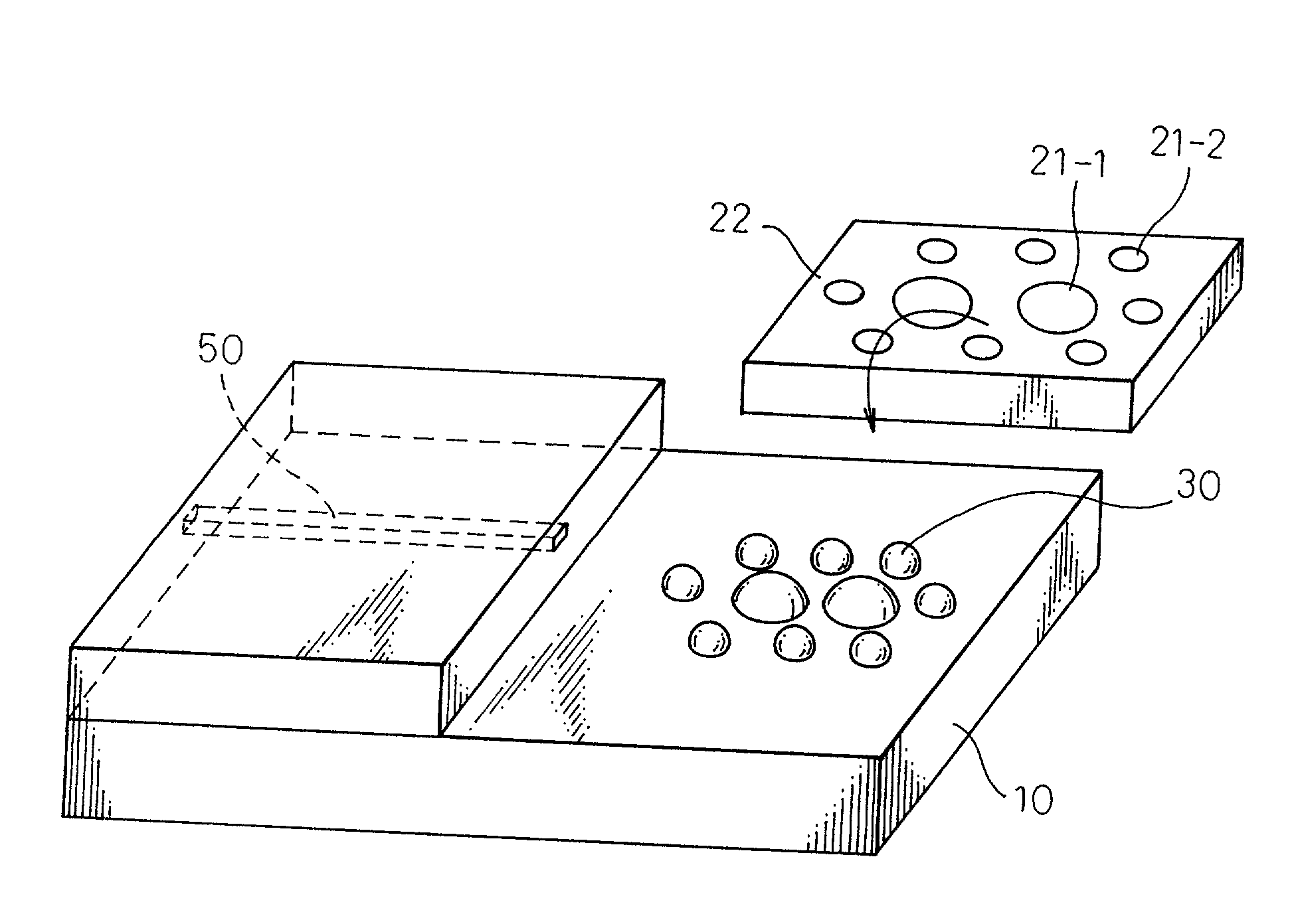
[0047] In the present example, a groove 12 is formed on a silicon substrate 10 based on anisotropic etching using an alkali etchant. Metal pads 11 are prepared such that the center of this groove 12 coincides with the centers of metal pads laid out on the optical axis on the substrate 10, in a similar manner to that of the first embodiment, as shown in FIGS. 9 and 10. In the present embodiment, all the metal pads 11 have diameters of 40 .mu.m, as in the example shown in FIG. 3. Therefore, large metal pads are not prepared on the substrate 10.

[0048] Next, solder consisting of Au by 80 weight % and Sn by 20 weight % is supplied to each pad, to have a thickness of 10 .mu.m and a diameter of 70 .mu.m for the solder, in a similar manner to that of the first embodiment. Flax is coated on the solder spots, and they are fused by heating, thereby to prepare solder bumps 30. When the metal pads for preparing the solder bumps 30 have the same diameters, the quantity of solder to be applied to ...

second embodiment

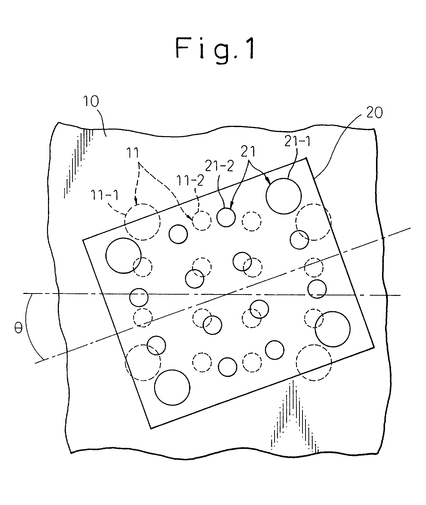
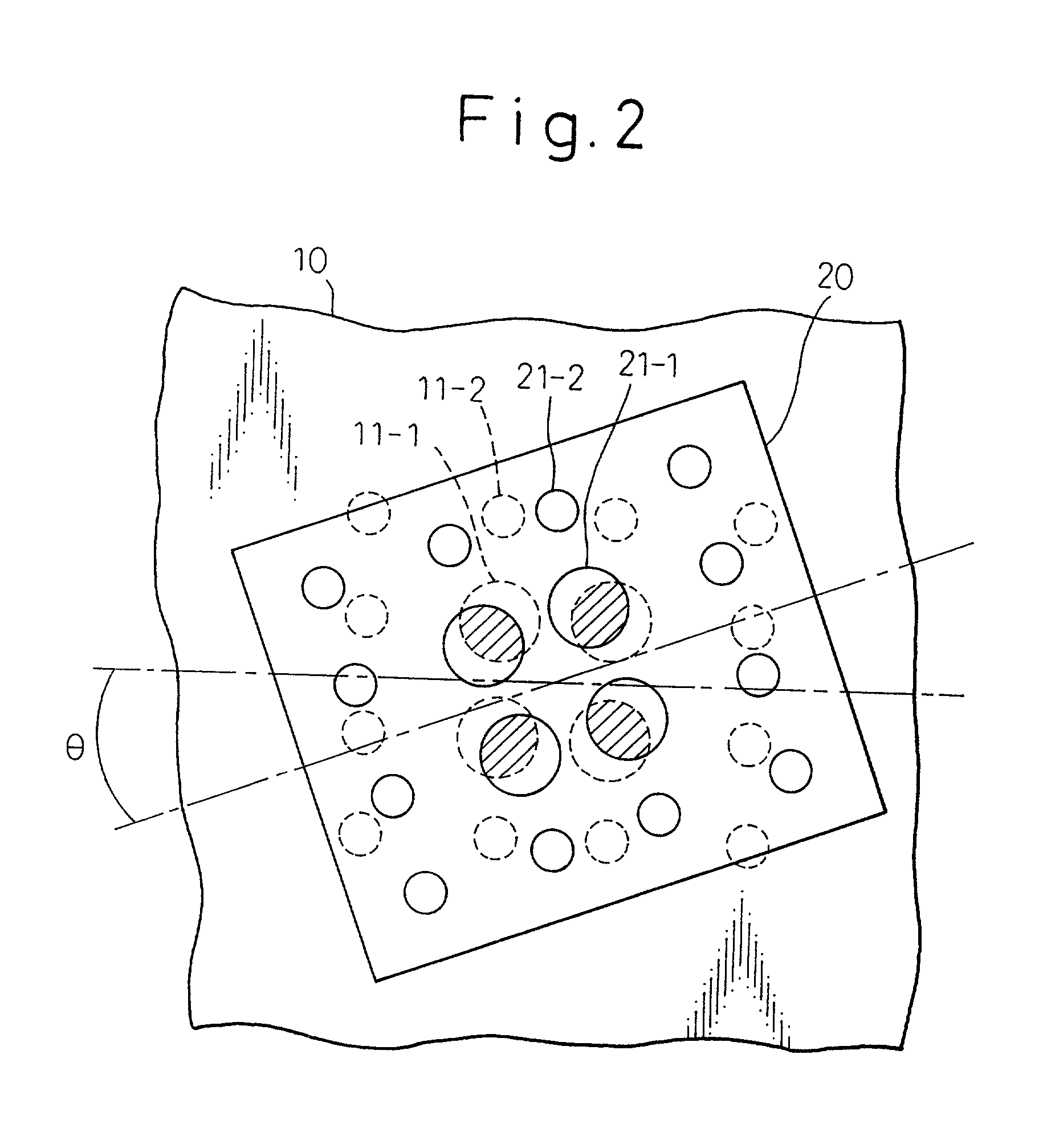
[0051] Last, an optical fiber 51 is engaged with the groove 12, so that the optical fiber 51 and the laser diode 22 are positioned together in high precision. Thus, fixed installation has been achieved. The present inventor has evaluated the positioning precision based on an experiment in a connection status similar to that of the As a result, it has been possible to obtain the mounting precision of 1 .mu.m or less in the final positioning based on the surface tension of the solder, when the large metal pads are in contact with the corresponding solder bumps at the time of the provisional mounting.

[0052] According to the above first and second embodiments, the angular deviation up to around 46 degrees has been permitted in the provisional positioning. However, the angular deviation only up to around 13 degrees has been permitted in the provisional positioning, when the installation has been carried out in the conventional structure that a laser diode having the same sizes of 300 .m...


PUM


Abstract

The invention relates to an installation technique for optical parts and electric parts. More particularly, it provides an installation structure and an installation method for optical modules that are applied to an optical communication field. The installation structure and the installation method can permit large tolerance of angular deviation in the provisional mounting, and can realize automatic positioning with high precision in the final mounting. The structure includes: a substrate on which a plurality of first metal pads are formed; a part to be mounted having second metal pads corresponding to the positions of the first metal pads; and solder bumps for connecting between the first and second metal pads to match the installation positions of these metal pads based on the surface tension of the solder bumps when the solder bumps are fused. In this structure, the substrate and/or the mounted part has at least two metal pads having larger areas than those of other metal pads, in the vicinity of the center of the substrate and/or the mounted part.

Description

[0001] This application is a continuation of PCT / JP99 / 04908.[0002] The present invention relates to an installation technique for optical parts and electric parts. More particularly, this invention relates to an installation structure and an installation method for optical modules that are used in the optical communication field.[0003] Conventionally, the positioning of an optical waveguide and an optical element has prevented cost reduction in the process of manufacturing an optical module. Particularly, accurate positioning in the order of micrometers (.mu.m) has been required to achieve an optical coupling between an optical waveguide and a laser diode (LD) as an optical element. As an installation method for easily carrying out this positioning, there is a self-alignment installation method for the positioning by utilizing the surface tension of solder.[0004] According to this installation method, a plurality of metal pads that become the basis of positioning are formed on a sub...

Claims


Application Information

Patent Timeline
IPC IPC(8): G02B6/42H01L21/60H01L23/498H05K1/11H05K3/34
CPCG02B6/4232H01L23/49838H01L2224/13144H01L2224/13111H01L2224/131H01L2924/014H01L2924/0105H01L2924/01033H01L2924/01006H01L2924/01005H05K2203/048H01L24/17H01L24/81H01L2224/13099H01L2224/81801H01L2924/01079H05K1/111H05K3/3436H05K2201/094H05K2201/09427H01L2924/00014H01L2924/01082H01L24/05H01L24/06H01L24/14H01L2224/0401H01L2224/05568H01L2224/05573H01L2224/056H01L2224/0603H01L2224/0615H01L2224/17051H01L2224/81143H01L2224/81192H01L2924/12042Y02P70/50H01L2924/00
Inventor NAKATA, HIDEHIKO
Owner FUJITSU LTD
Why Eureka
Try Eureka