Wiring substrate, wiring board, and wiring substrate mounting structure

Inactive Publication Date: 2002-06-20
KYOCERA CORP
View PDF13 Cites 29 Cited by
  • Summary
  • Abstract
  • Description
  • Claims
  • Application Information

AI Technical Summary

Problems solved by technology

Consequently, the wiring board has been conventionally fabricated using a low-loss material havin

Method used


Image

  • Wiring substrate, wiring board, and wiring substrate mounting structure
  • Wiring substrate, wiring board, and wiring substrate mounting structure
  • Wiring substrate, wiring board, and wiring substrate mounting structure

Examples


Embodiment Construction

[0060] The following experiments were conducted in order to confirm the effect of the present invention.

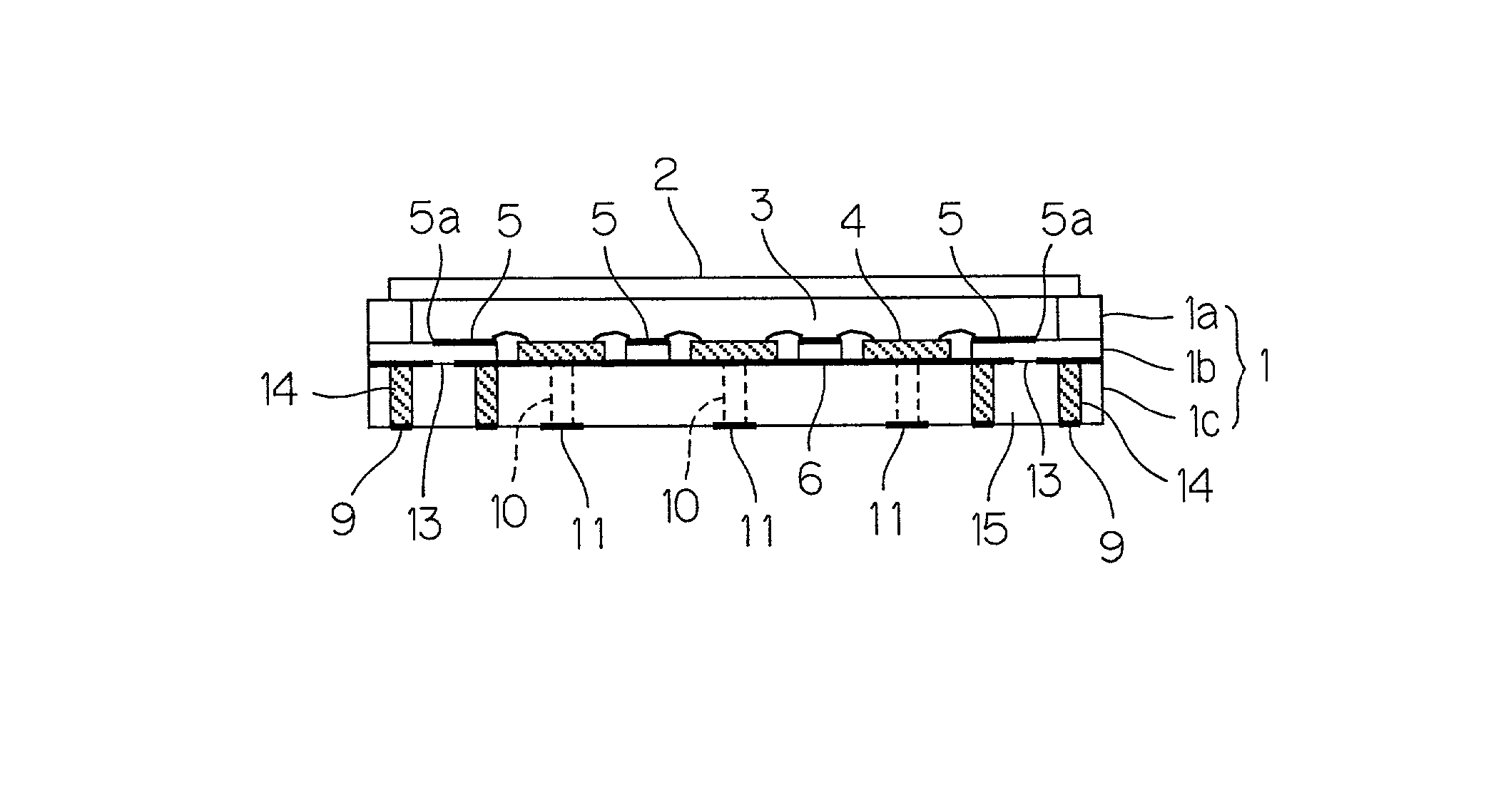
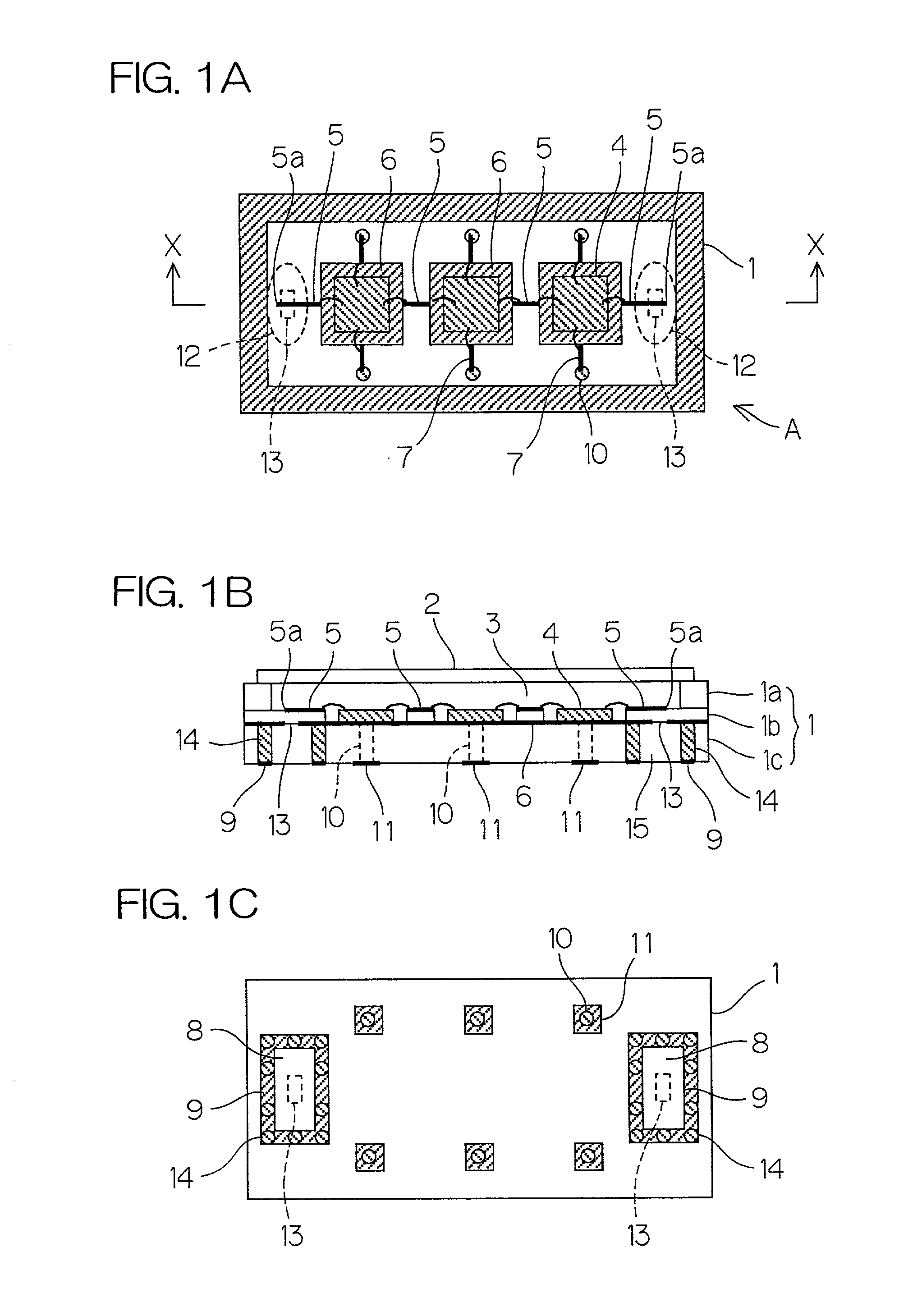
[0061] First, as a wiring substrate A, a substrate for evaluation which is similar to the wiring substrate A shown in FIG. 1 was fabricated by a normal stacking and simultaneous sintering technique using a green sheet composed of alumina ceramics (if the green sheet is sintered, the dielectric loss tangent at a frequency of 10 GHz is 0.0006) and tungsten metallized ink.

[0062] In the substrate for evaluation, there is no cavity in the wiring substrate A shown in FIG. 1, no high frequency component is carried thereon, and two microstrip lines each having an opened terminal end for input and output signals are connected to each other. An example of a matching section was one having a structure of a microstrip line 5, a slot hole 13, and a matching section 15 as shown in FIGS. 1A to 1C. After sintering, metallized surfaces of a surface and a reverse surface of a dielectric substrate w...


PUM


Abstract

In a wiring substrate, a high-frequency component is carried on a dielectric board having a transmission line formed on its surface, a reverse surface of the dielectric board is formed with an opening in a predetermined cross-sectional shape, and a high-frequency connecting pad is formed around the opening. In the wiring board, a dielectric board penetrates a waveguide structure and has its inner wall coated with a conductor, and a high-frequency connecting pad is formed on a surface of the dielectric board. The wiring substrate is placed on the wiring board, and the respective high-frequency connecting pads are electrically connected to each other, to fabricate a module. Even when a low-cost material having a large dielectric loss tangent is used for the wiring board, a high-frequency signal can be prevented from being attenuated.

Description

[0001] This application is based on application No. 2000-361749 filed in Japan, the content of which is incorporated hereinto by reference.[0002] 1. Field of the Invention[0003] The present invention relates to a wiring substrate used in a microwave region or a millimeter wave region, a wiring board, and a wiring substrate mounting structure.[0004] 2. Description of the Related Art[0005] It has been examined whether or not an electric wave is made use of for transmitting information from a microwave region of 1 to 30 GHz to a millimeter wave region of 30 to 300 GHz. An electric wave application system using a millimeter electric wave, for example, a radar between vehicles has been put to practical use.[0006] As an example of electric components using such high frequencies, a wiring substrate accommodating a plurality of chips in its one case is assumed.[0007] FIG. 6 is a schematic sectional view for explaining the structure of such a wiring substrate 60. In FIG. 6, a metal case 61 a...

Claims


Application Information

Patent Timeline
IPC IPC(8): H01L23/12H01L23/14H01L23/66H01L25/04H01L25/10H01L25/11H01L25/18H05K1/02H05K3/42
CPCH01L23/66H01L2223/6627H01L2224/45144H01L24/49H01L2924/01087H01L2924/01019H01L24/48H05K2201/10734H01L2224/48091H01L2224/48227H01L2224/49175H01L2924/01039H01L2924/01078H01L2924/01079H01L2924/09701H01L2924/15153H01L2924/1517H01L2924/16152H01L2924/16195H01L2924/1903H01L2924/19041H01L2924/3011H05K1/0243H05K1/0272H05K3/429H05K2201/09854H05K2201/10545H05K2201/10727H01L2924/00014H01L2924/00H01L2924/30111H01L24/45H01L2924/00015
Inventor KORIYAMA, SHINICHI
Owner KYOCERA CORP
Why Eureka
Try Eureka