Light emitting diode and method of making the same

a technology of light-emitting diodes and diodes, which is applied in the field of optoelectronic devices, can solve the problems of limiting the usefulness of this type, internal reflections that do not provide directed light output or parallel beams, and achieve the effect of improving light-emitting efficiency

Inactive Publication Date: 2002-08-08
INTERUNIVERSITAIR MICRO ELECTRONICS CENT (IMEC VZW) +1
View PDF0 Cites 24 Cited by
  • Summary
  • Abstract
  • Description
  • Claims
  • Application Information

AI Technical Summary

Benefits of technology

0008] It is an object of the present invention to provide an opto-electronic device with improved light output efficiency.

Problems solved by technology

Unfortunately, due to the resonance, output efficiency and directionality depend quite strongly on the temperature, limiting the usefulness of this type of LED to some niche applications and markets.
These LED's with multiple internal reflection don't provide a directed light output or a parallel beam.

Method used


Image

  • Light emitting diode and method of making the same
  • Light emitting diode and method of making the same
  • Light emitting diode and method of making the same

Examples


first embodiment

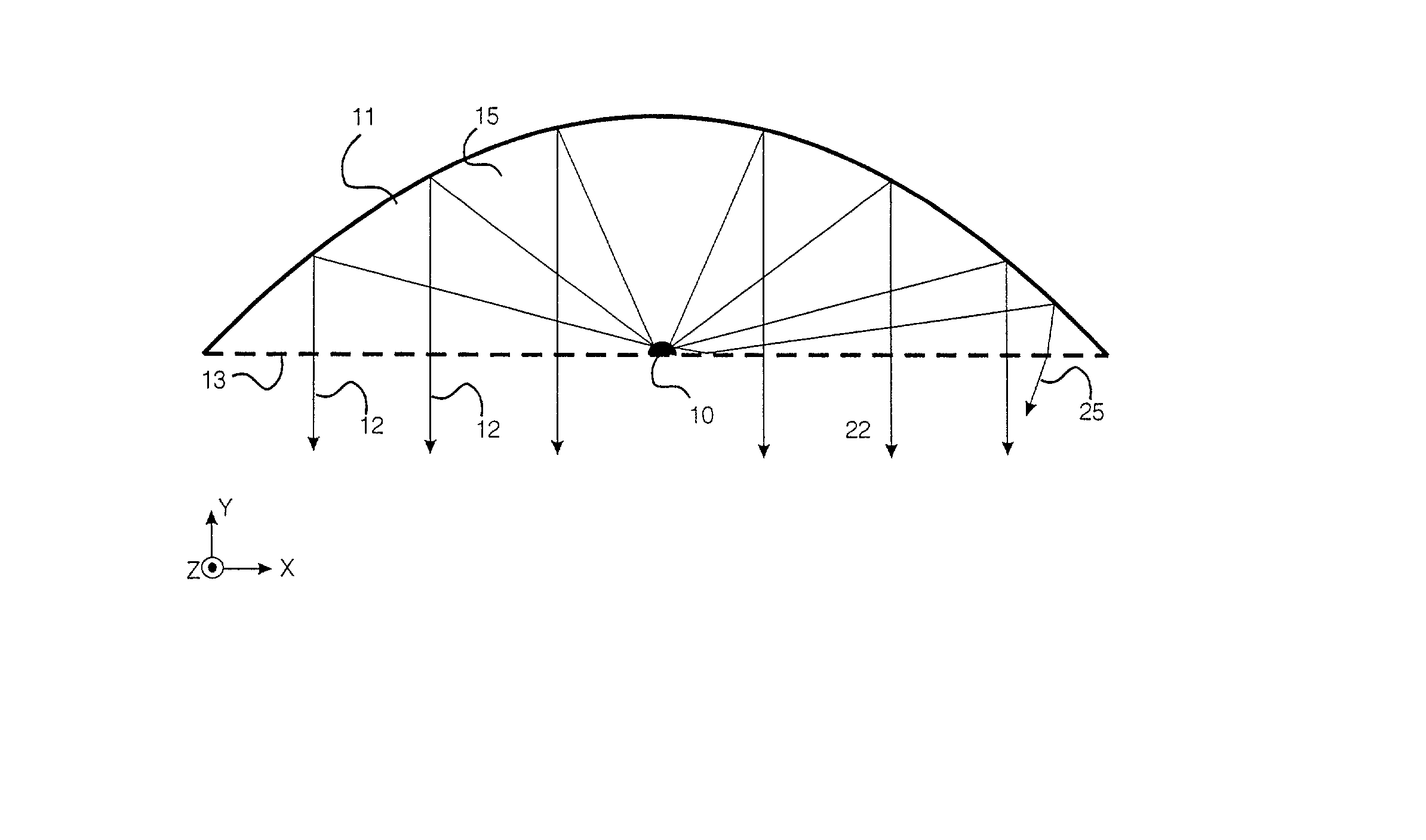
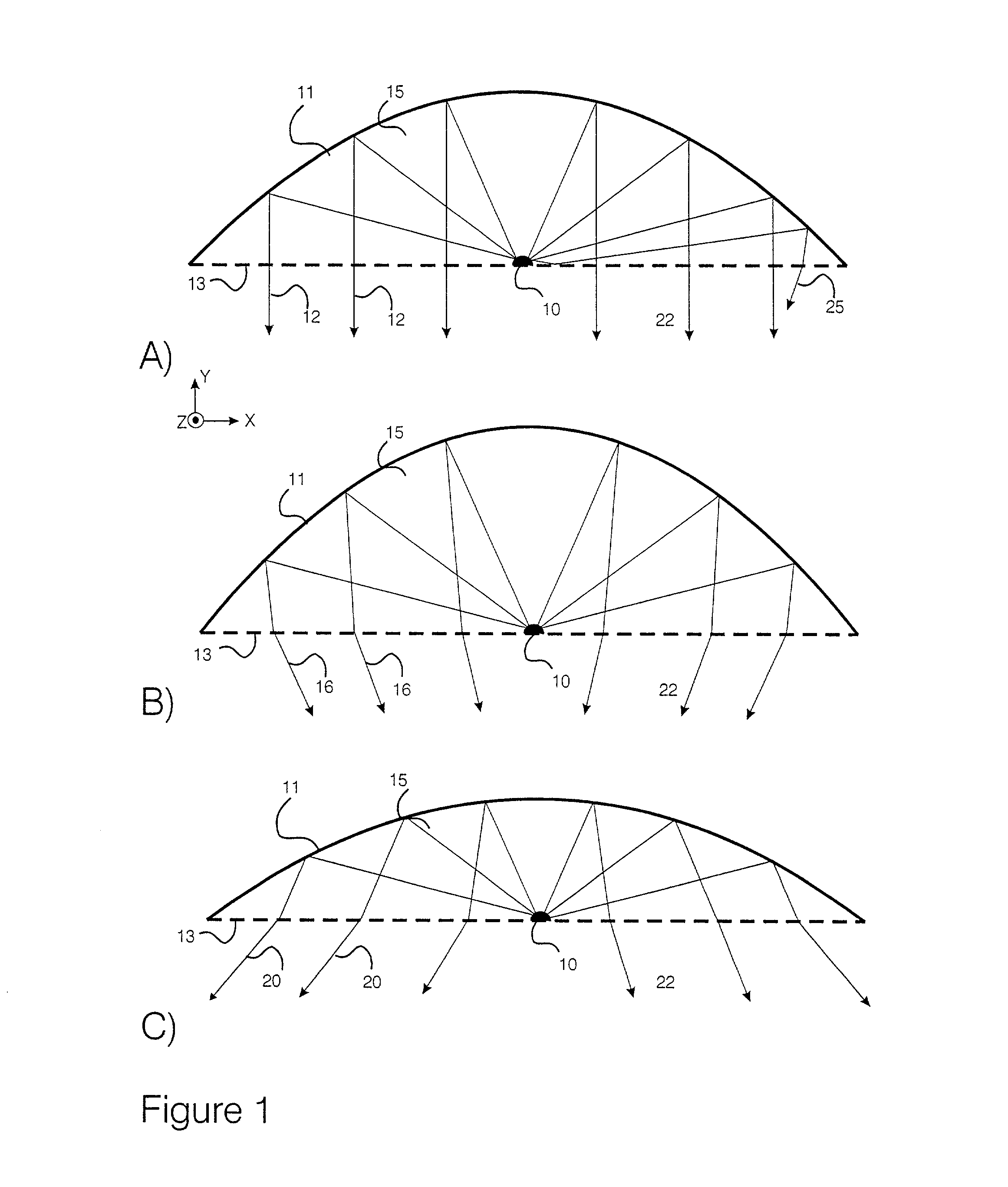
[0035] FIGS. 1A to 1C are schematic views of an opto-electronic device according to the present invention. The opto-electronic device may be an LED comprising a body of material (15), preferably of semiconductor material, having a radiation generating zone (10). Light or electromagnetic radiation generated in this radiation generating zone (10) will be emitted in all directions as illustrated in FIG. 1A by the arrows (12). Preferably, the zone is spatially confined. For the purposes of simplification of this description only this radiation generating zone (10) is so small that it can be considered as a single point from which light is emitted. The generation of light should preferably be confined or limited in space to avoid production of light outside the immediate vicinity of the focal point of a reflector surface (11). A portion of the surface of the semiconductor material (15) has a spherical shape or is shaped as a conic of revolution, e.g. a paraboloid, a hyperboloid. This por...

second embodiment

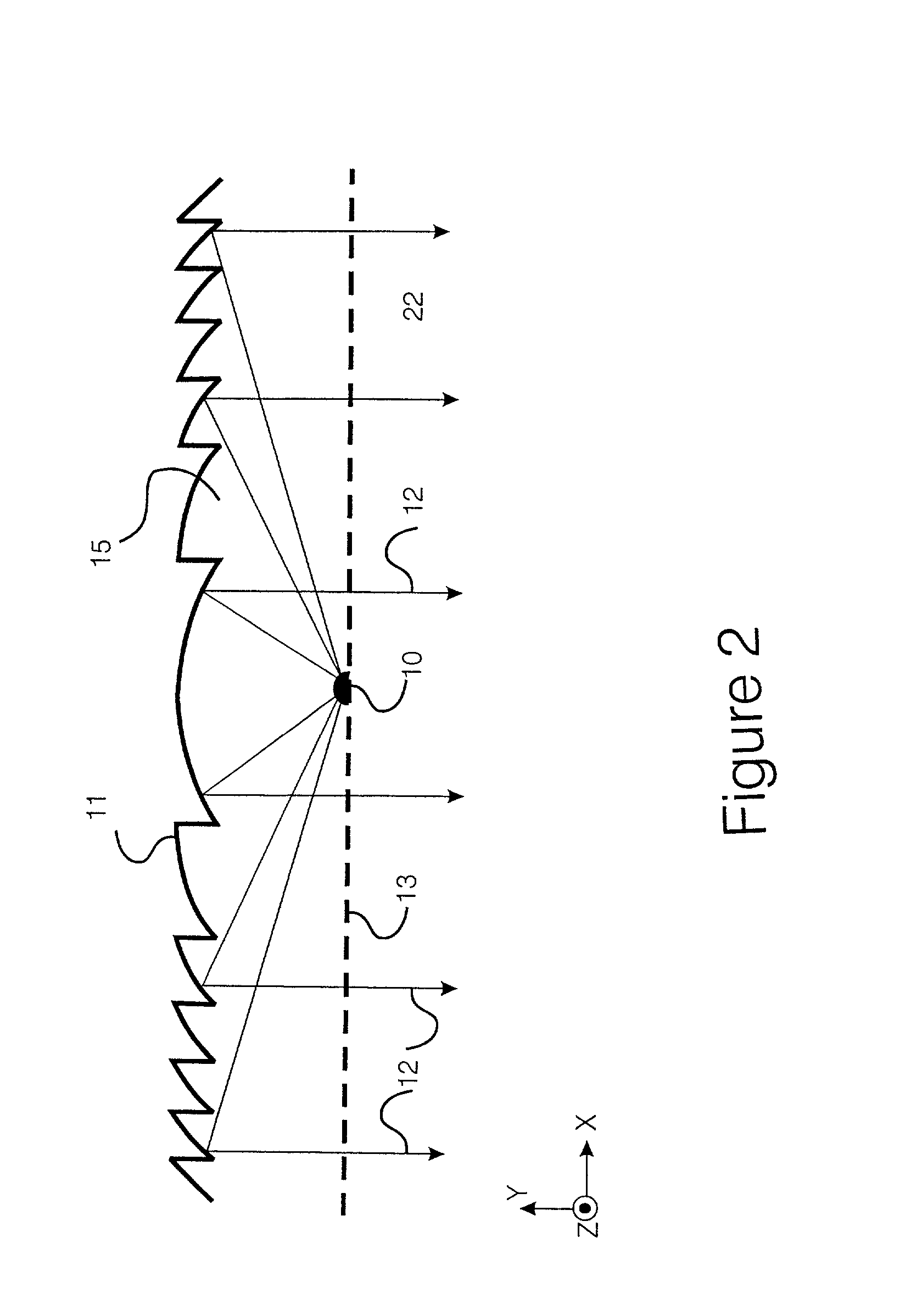
[0042] In a second embodiment an alternative to a parabolic shaped reflector (11) is given. Such an alternative can be a Fresnel type of reflector as shown in FIG. 2. It is known to a person skilled in the art that most lenses have a Fresnel equivalent. Similarly, reflectors can have a Fresnel equivalent. Gray-scale mask technology allows the manufacturing of such equivalent structures, as will be explained in further embodiments. Also in case of a Fresnel equivalent reflector the light generation is preferably confined to a region (10) located as much as possible at the focal point of the constructed equivalent reflector. The reflecting properties of the reflecting surface (11) can also be improved by depositing a dielectric and metallic layer, as will be illustrated in further embodiments. Rays (12) can be made focussing (convergent) or defocusing (divergent), according to the design specifications, by changing the relative position of the radiation generation zone (10) and the ou...

third embodiment

[0043] In a third embodiment another alternative to a semispherical, concave or parabolic shaped reflector (11) is provided. As illustrated in FIG. 3 the radiating surface (13) can be made semi-spherical or in the form of a conic of revolution and the reflecting surface (11) can be substantially planar. The light generation zone (10) is located adjacent to the out-couple surface (13) at a symmetry axis of the device.

[0044] In a second aspect of the present invention methods of manufacturing devices according the present invention are given.


PUM


Abstract

The present invention discloses a highly efficient light emitting diode with directional properties comprising a light cavity of semiconductor material. A portion of the surface of the light cavity acts as a parabolic shaped reflector. A light generation zone is located substantially at the focal point of this paraboloid reflector. The light out-coupling interface of the cavity is close to the focal point allowing both downward and upward generated photons to escape from the semiconductor cavity. Photons reach the out-coupling interface in perpendicular way within the out-coupling cone of the semiconductor-surrounding medium interface.

Description

[0001] This application claims priority to co-pending U.S. provisional patent application titled "HIGHLY EFFICIENT PARABOLOID LED", having Application No. 60 / 259,798, and filed on Jan. 4, 2001.[0002] The present invention relates to a light emitting opto-electronic components comprising a semiconductor body and methods of making the same, especially light emitting diodes suitable for use as opto-couplers or opto-telecommunications applications.[0003] A need exists for highly efficient Light Emitting Diodes (LED's) for applications in data communication as well as for illumination purposes. A Light Emitting Diode normally comprises a semiconductor part wherein the light is generated, means to supply current to this semiconductor part and a medium surrounding the semiconductor part. The external efficiency of such LED depends not only on the amount of light generated within the semiconductor part of the device, but also on the amount of this generated light that is being emitted by th...

Claims


Application Information

Patent Timeline
Patent Type & Authority Applications(United States)
IPC IPC(8): H01L27/15H01L33/10H01L33/20
CPCH01L27/153H01L27/156H01L33/10H01L33/20
Inventor KUIJK, MAARTENHEREMANS, PAUL
Owner INTERUNIVERSITAIR MICRO ELECTRONICS CENT (IMEC VZW)
Why Eureka
Try Eureka