Semiconductor chip having an arrayed waveguide grating and method of manufacturing the semiconductor chip and module containing the semiconductor chip

a technology of semiconductor chips and waveguide gratings, which is applied in the field of semiconductor chips, can solve the problems of low wafer utilization efficiency

Inactive Publication Date: 2002-08-22
NEC CORP
View PDF0 Cites 15 Cited by
  • Summary
  • Abstract
  • Description
  • Claims
  • Application Information

AI Technical Summary

Problems solved by technology

Consequently, when arrayed waveguide gratings are cut out as rectangular chips as in the related art, wafer utilizat

Method used


Image

  • Semiconductor chip having an arrayed waveguide grating and method of manufacturing the semiconductor chip and module containing the semiconductor chip
  • Semiconductor chip having an arrayed waveguide grating and method of manufacturing the semiconductor chip and module containing the semiconductor chip
  • Semiconductor chip having an arrayed waveguide grating and method of manufacturing the semiconductor chip and module containing the semiconductor chip

Examples


Embodiment Construction

[0033] Hereinafter, the present invention will be described in detail with reference to the drawings.

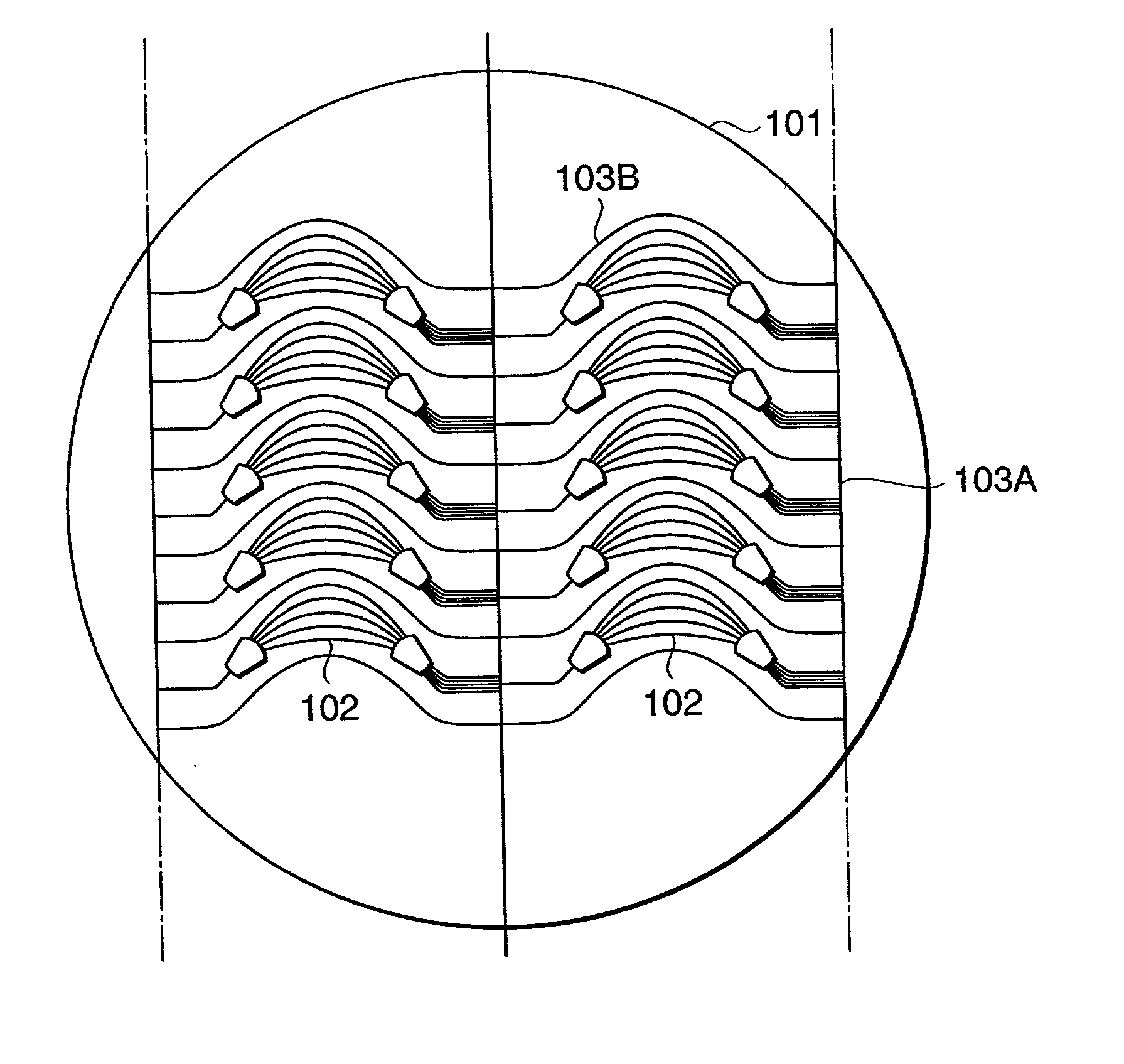
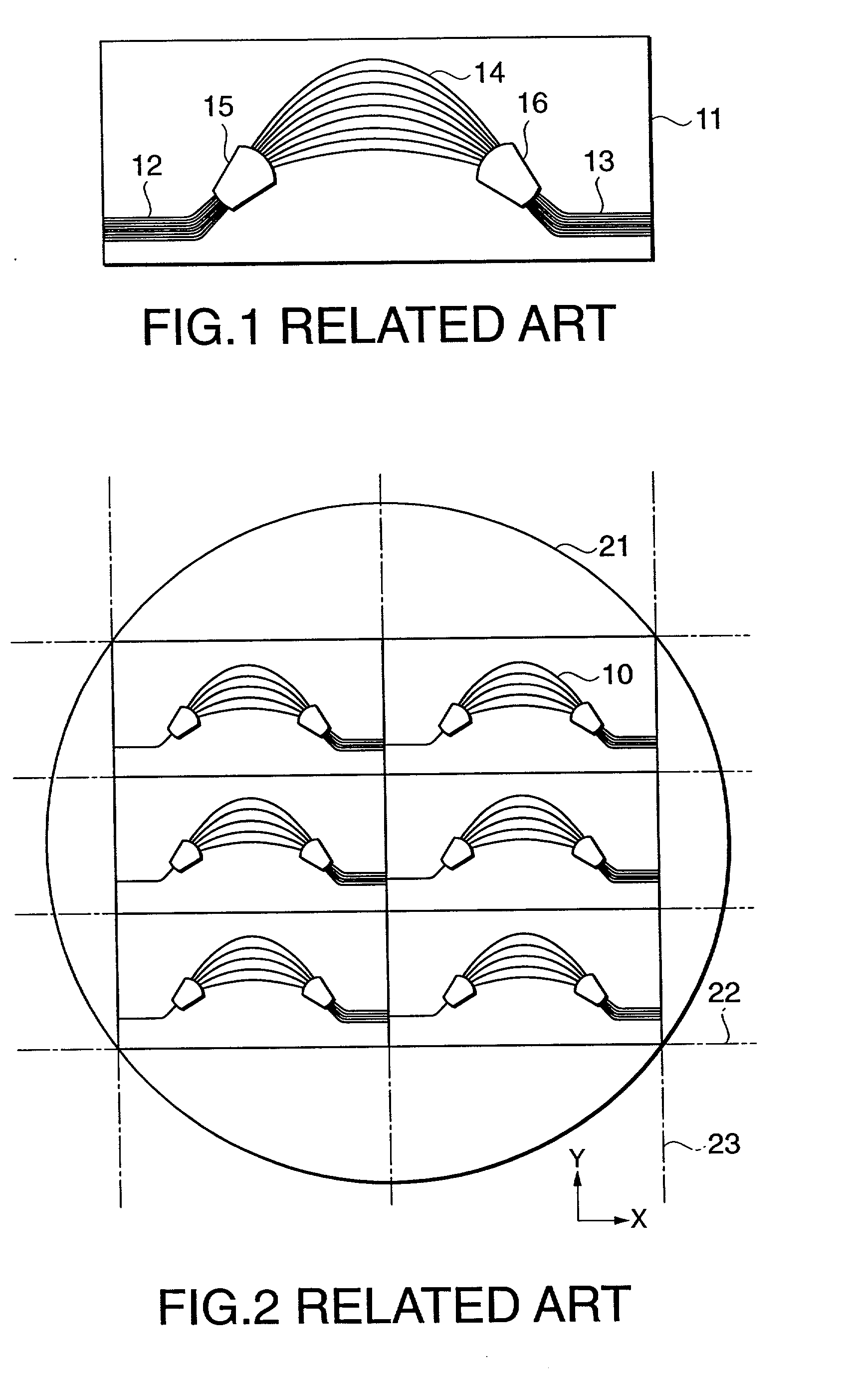
[0034] FIG. 4 shows arrayed waveguide grating elements formed on a wafer according to the present invention. In FIG. 4, each arrayed waveguide grating 102 has a shape similar to the shape shown in FIG. 1. Five arrayed waveguide gratings 102 are formed in one row. Thus, ten arrayed waveguide gratings 102 are formed in total. In each arrayed waveguide grating 102, the portion corresponding to the channel waveguide array 14 (shown in FIG. 1) is curved into an arcuate shape. Cutting paths 103A and 103B for cutting out an individual arrayed waveguide grating chip are scribed so as to surround each of the arcuate or typical boomerang-shaped portions of the arrayed waveguide gratings 102. The cutting paths 103 comprise straight cutting paths 103A and curved cutting paths 103B. For the cutting paths 103B, two arcuate portions of the same shape are arranged side by side in a lateral direction...


PUM

PropertyMeasurementUnit
Temperatureaaaaaaaaaa
Pressureaaaaaaaaaa
Shapeaaaaaaaaaa

Abstract

On a wafer, patterns of arrayed waveguide gratings are formed. Each arrayed waveguide grating has an arcuate shape obtained by arranging two curved-line portions convexed in the same direction at a predetermined spacing and connecting respective end portions thereof with two mutually parallel straight lines. These arrayed waveguide gratings are cut out along straight cutting paths and curved cutting paths in which two arcuate portions of the same shape are arranged side by side in a lateral direction. Thus, a larger number of chips can be produced as compared with a case where each array waveguide grating is cut out in a rectangular shape. Ultrasonic machining techniques or sandblast machining techniques are suitable for the cutting operation.

Description

[0001] 1. Field of the Invention[0002] The present invention relates to a semiconductor chip obtained by cutting, from a wafer, an element occupying a non-rectangular area. The present invention also relates to a module containing an element occupying a nonrectangular area. For example, the present invention relates to a chip and a manufacturing method thereof such as an arrayed waveguide grating chip, a manufacturing method thereof, and manufacturing a module containing an arrayed waveguide grating chip.[0003] 2. Description of the Related Art[0004] As the volume of data to be transmitted increases, there is a corresponding demand for a larger transmission capacity in an optical fiber communications system. In addition, optical wavelength filtering is becoming increasingly important as an optical multiplexing / demultiplexing device for multiplexing and / or demultiplexing different wavelengths in Dense Wavelength Division Multiplexing (DWDM) systems. There are various types of optical...

Claims


Application Information

Patent Timeline
IPC IPC(8): B23K20/10G02B6/12B23K26/38B23K26/40B23K101/40B24C1/00B26F3/00B26F3/04G02B6/13G02B6/30G02B6/34
CPCG02B6/12007G02B6/12021G02B6/12026G02B6/12033G02B6/125G02B6/13G02B6/29353G02B6/30
Inventor WATANABE, SHINYAKATOU, HIROYUKI
Owner NEC CORP
Why Eureka
Try Eureka