Method of forming color filter array

a color filter array and color technology, applied in the field of forming optical devices, can solve the problems of poor light absorption of silicon oxynitride layer, inability to absorb reflected light, and the conventional method of fabricating color filter arrays has several problems, so as to improve the final quality of patterned color filter arrays and improve the resolution of photolithographic processes. , the effect of improving the light absorption capacity

Inactive Publication Date: 2002-09-12
UNITED MICROELECTRONICS CORP
View PDF0 Cites 6 Cited by
  • Summary
  • Abstract
  • Description
  • Claims
  • Application Information

AI Technical Summary

Benefits of technology

[0013] In the aforementioned photolithographic exposure, a light source having a wavelength less than or equal to 248 nm is used in photolithographic exposure. Since silicon oxynitride material has a higher light absorption capacity for light at such a wavelength, the passivation layer actually serves also as an anti-reflection coating that improves the final quality of the patterned color filter array.
[0014] In addition, by using a light source having a wavelength less than or equal to 248 nm rather than an i-line light source, resolution of the photolithographic process is increased. Ultimately, both area utilization and resolution of the color filter panel improves.

Problems solved by technology

However, the conventional method of fabricating a color filter array has several problems.
However, the silicon oxynitride layer is a poor absorber for light of this wavelength and hence cannot absorb reflected light 132a coming from a lower layer.
Ultimately, image quality of the device will deteriorate.
Second, the conventional method of forming a blue color filter array often leads to color pixel peeling due to insufficient light exposure. FIGS. 2A and 2B are schematic cross-sectional views showing a conventional technique for forming a blue color filter array on a substrate and resulting adverse consequence.
In addition, resolution of a light source with a wavelength of 365 nm is relatively low and hence area utilization is unsatisfactory.
Furthermore, resolution of the color filters is ultimately limited by the resolution of the light source.

Method used


Image

  • Method of forming color filter array
  • Method of forming color filter array
  • Method of forming color filter array

Examples


Embodiment Construction

[0021] Reference will now be made in detail to the present preferred embodiments of the invention, examples of which are illustrated in the accompanying drawings. Wherever possible, the same reference numbers are used in the drawings and the description to refer to the same or like parts.

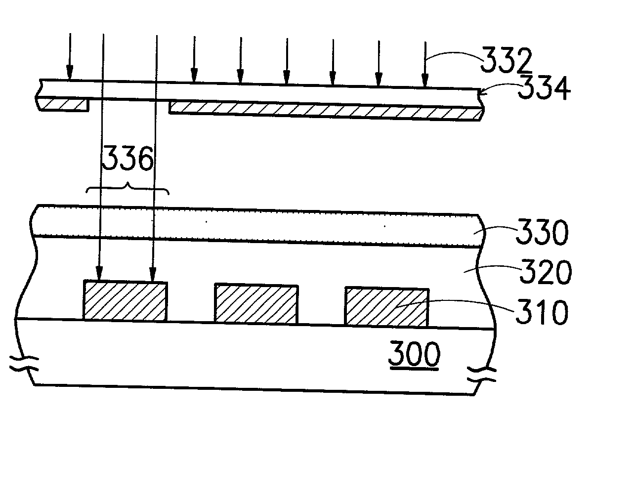
[0022] FIGS. 3A through 3C are schematic cross-sectional views showing the progression of steps for fabricating a tricolor filter array according to a preferred embodiment of this invention.

[0023] As shown in FIG. 3A, a substrate 300 having an array of metallic elements 310 thereon is provided. The array of metallic elements 310 serves light sensors so that a current is produced and delivered to a detector when a light impinges upon the metallic elements 310. A passivation layer 320 is formed over the substrate 300 and the metallic elements 310. The passivation layer 320 can be a silicon oxynitride layer having a thickness greater than 1000 .ANG.. A negative color photoresist layer 330 that permits ...


PUM

PropertyMeasurementUnit
wavelengthaaaaaaaaaa
thicknessaaaaaaaaaa
wavelengthaaaaaaaaaa

Abstract

A method of forming a color filter array. A substrate having a passivation layer thereon is provided. A negative color photoresist layer is formed over the passivation layer. A photolithographic exposure process is conducted using a light source with a wavelength less than or equal to 248 nm so that a pattern for forming a color filter array is imprinted on the negative color photoresist layer.

Description

BACKGROUND OF THE INVENTION[0001] 1. Field of Invention[0002] The present invention relates to a method of forming an optical device. More particularly, the present invention relates to a method of forming a color filter array (CFA).[0003] 2. Description of Related Art[0004] Color filter array (CFA) is frequently used in optical devices for displaying color images. In such an optical device, each pixel generally corresponds to three neighboring but different color filters. In other words, a specified color is permitted to pass through each filter. A complete color palette can be obtained, for example, by mixing the colors from the three filters such as red (R), green (G) and blue (B). Therefore, the pixel array in an image display device actually consists of an array of three types of color filters such as an array of red filters, an array of green filters and an array of blue filters.[0005] The fabrication of an optical device that displays colorful images normally involves forming...

Claims


Application Information

Patent Timeline
Patent Type & Authority Applications(United States)
IPC IPC(8): G02B5/20G03F7/00
CPCG02B5/201G03F7/0007
Inventor CHEN, JAIN-HONYEH, JEENH-BANG
Owner UNITED MICROELECTRONICS CORP
Why Eureka
Try Eureka