Multilevel interconnect structure containing air gaps and method for making

a technology of air gaps and interconnect structures, which is applied in the direction of electrical equipment, semiconductor devices, semiconductor/solid-state device details, etc., can solve the problems of affecting chip speed, and thus chip performance, and the air gap structure may not be as uniformly planar, so as to minimize the amount of unsupported wiring, maximize the air gap volume fraction, and cost-effective and scalable

Inactive Publication Date: 2002-09-12
GLOBALFOUNDRIES US INC
View PDF9 Cites 143 Cited by
  • Summary
  • Abstract
  • Description
  • Claims
  • Application Information

AI Technical Summary

Benefits of technology

0016] Another object of the present invention is to provide an air gap-containing interconnect structure which maximizes air gap volume fraction (relative to total volume fraction of dielectric), while minimizing the amount of unsupported wiring.
0017] A still further object of the present invention is to provide a cost-effective and scalable method for fabricating multilevel interconnect structures having air gaps.
0018] An even further object of the present invention is to, provide a method for-forming air gap-containing interconnect structures which minimizes the amount of processing that air gaps in the structure will experience during the fabrication of the structure.
0019] Another object of t

Problems solved by technology

By means of their effects on signal propagation delays, the materials and layout of these interconnect structures can substantially impact chip speed, and thus chip performance.
A further concern with air gap dielectrics is that they leave metal wiring features more susceptible to the opens and shorts induced by electromigration-driven mass transport, since the wiring features are no longer dimensionally constrained by being embedded in

Method used


Image

  • Multilevel interconnect structure containing air gaps and method for making
  • Multilevel interconnect structure containing air gaps and method for making
  • Multilevel interconnect structure containing air gaps and method for making

Examples


Embodiment Construction

[0037] The present invention which provides methods of fabricating a multilevel interconnect structure having air gaps therein as well as a multilevel interconnect structure will now be described in more detail by referring to the following description as well as the drawings that accompany the present application.

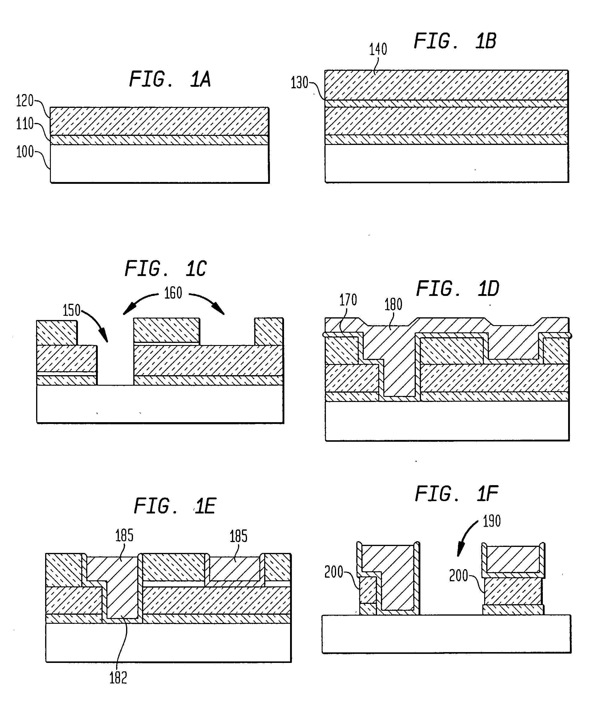
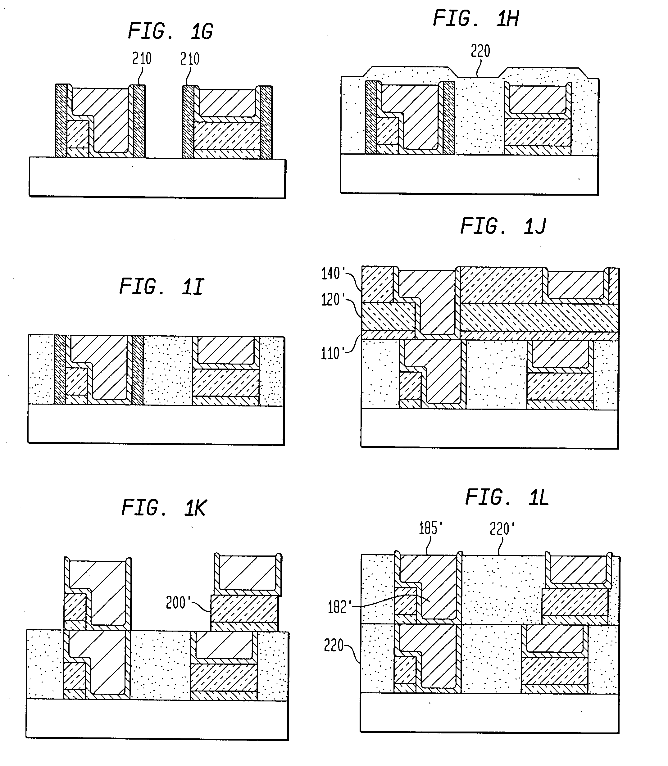
[0038] Reference is first made to FIGS. 1A-1P which show, in cross section view, the basic steps of the instant invention for forming an air-gap containing interconnect structure. Specifically, FIG. 1A comprises substrate 100 (which would normally comprise devices interspersed with conductive regions and insulating regions) after the application of optional dielectric etch stop / barrier / adhesion layer 110 and dielectric layer 120 having a combined thickness approximately equal to the desired via level thickness. FIG. 1B shows the structure after deposition of an optional dielectric etch stop / barrier / adhesion layer 130, and line level dielectric 140. Line level dielectric 14...


PUM


Abstract

A method for forming a multilayer interconnect structure on a substrate that include interconnected conductive wiring and vias spaced apart by a combination of solid or gaseous dielectrics. The inventive method includes the steps of: (a) forming a first planar via plus line level pair embedded in a dielectric matrix formed from one or more solid dielectrics and comprising a via level dielectric and a line level dielectric on a substrate, wherein, at least one of said solid dielectrics is at least partially sacrificial; (b) etching back sacrificial portions of said at least partially sacrificial dielectrics are removed to leave cavities extending into and through said via level, while leaving, at least some of the original via level dielectric as a permanent dielectric under said lines; (c) partially filling or overfilling said cavities with a place-holder material which may or may not be sacrificial; (d) planarizing the structure by removing overfill of said place-holder material; (e) repeating, as necessary, steps (a)-(d); (f) forming a dielectric bridge layer over the planar structure; and (g) forming air gaps by at least partially extracting said place-holder material.

Description

CROSS REFERENCE TO RELATED APPLICATIONS[0001] Cross reference is made to U.S. application Ser. No. 09 / 374,839, filed Aug. 14, 1999 by Clevenger, et-al. entitled "Semi Sacrificial Diamond for Air Dielectric Formation" and to U.S. application Ser. No. 09 / 112,919, filed Jul. 9, 1998 by T. O. Graham, et al. entitled "A Chip Interconnect Wiring Structure with Low Dielectric Constant Insulator and Methods for Fabricating the Same," both directed towards multilevel interconnect structures on integrated circuit chips incorporating a gaseous dielectric medium in at least one level, confined to within the chip by a dielectric encapsulate.FIELD OF THE INVENTION[0002] The present invention relates to air gap-containing metal / insulator interconnect structures for Very Large Scale Integrated (VLSI) and Ultra-Large Scale Integrated (ULSI) devices and packaging, and more particularly to structures, methods, and materials relating to the incorporation of air gaps into multiple levels of multilayer i...

Claims


Application Information

Patent Timeline
IPC IPC(8): H01L21/768
CPCH01L21/7682H01L21/76831H01L21/76834H01L21/76835H01L21/76885
Inventor GRILL, ALFREDHEDRICK, JEFFREY CURTISJAHNES, CHRISTOPHER VINCENTNITTA, SATYANARAYANA VENKATAPETRARCA, KEVIN S.PURUSHOTHAMAN, SAMPATHSAENGER, KATHERINE LYNNWHITEHAIR, STANLEY JOSEPH
Owner GLOBALFOUNDRIES US INC
Why Eureka
Try Eureka