

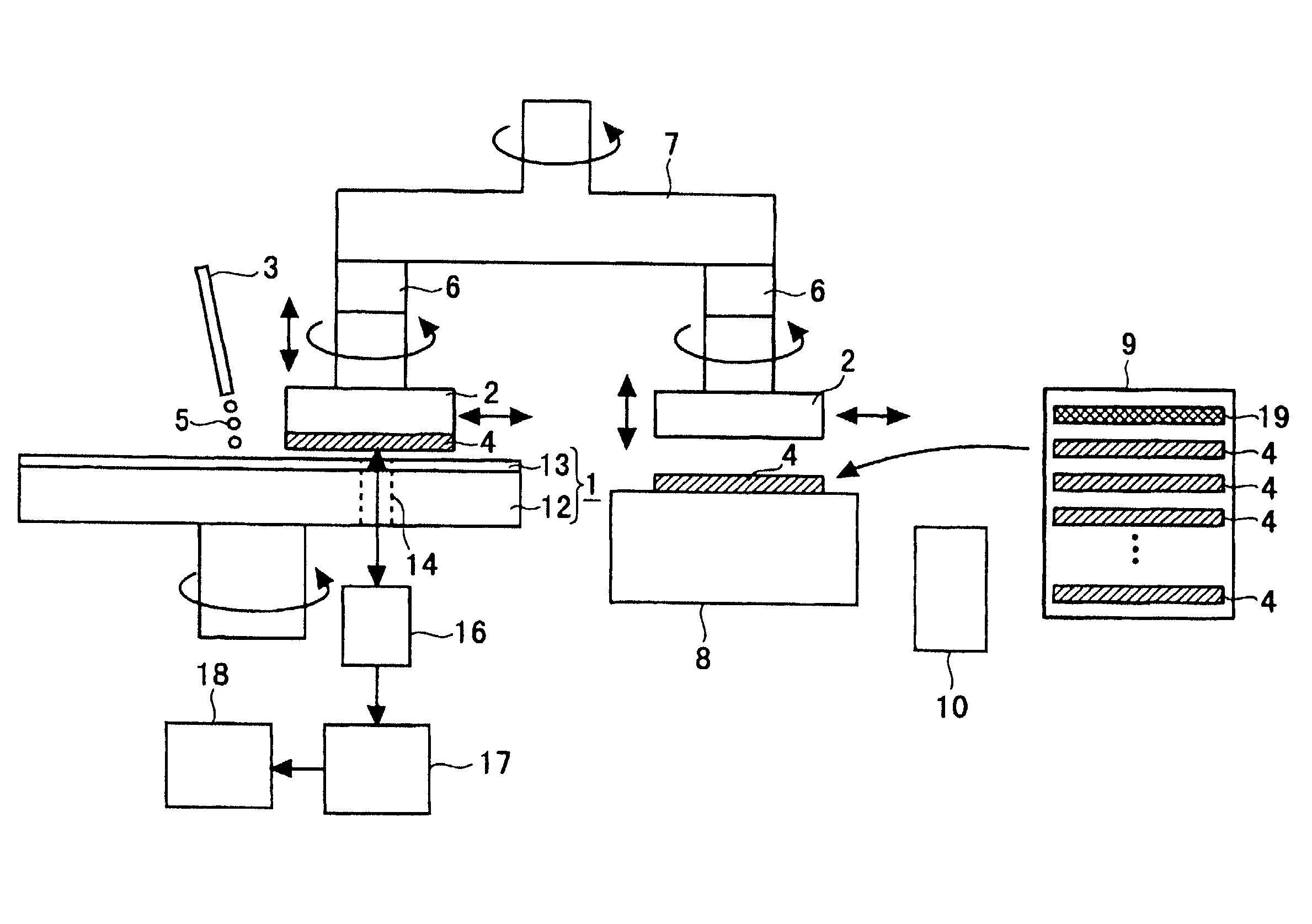
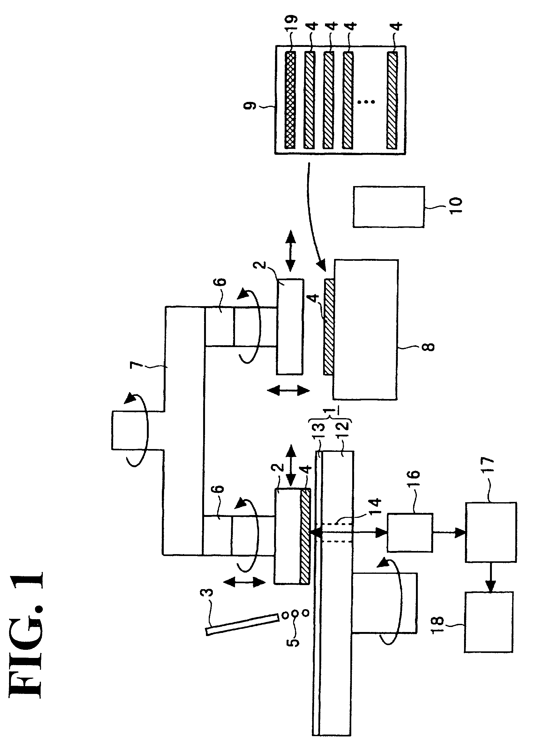
Method and apparatus for monitoring polishing state, polishing device, process wafer, semiconductor device, and method of manufacturing semiconductor device
a polishing state and polishing technology, applied in the direction of manufacturing tools, lapping machines, instruments, etc., can solve problems such as nois
- Summary
- Abstract
- Description
- Claims
- Application Information
AI Technical Summary
Benefits of technology
Problems solved by technology
Method used
Image

Examples
experimental example 2
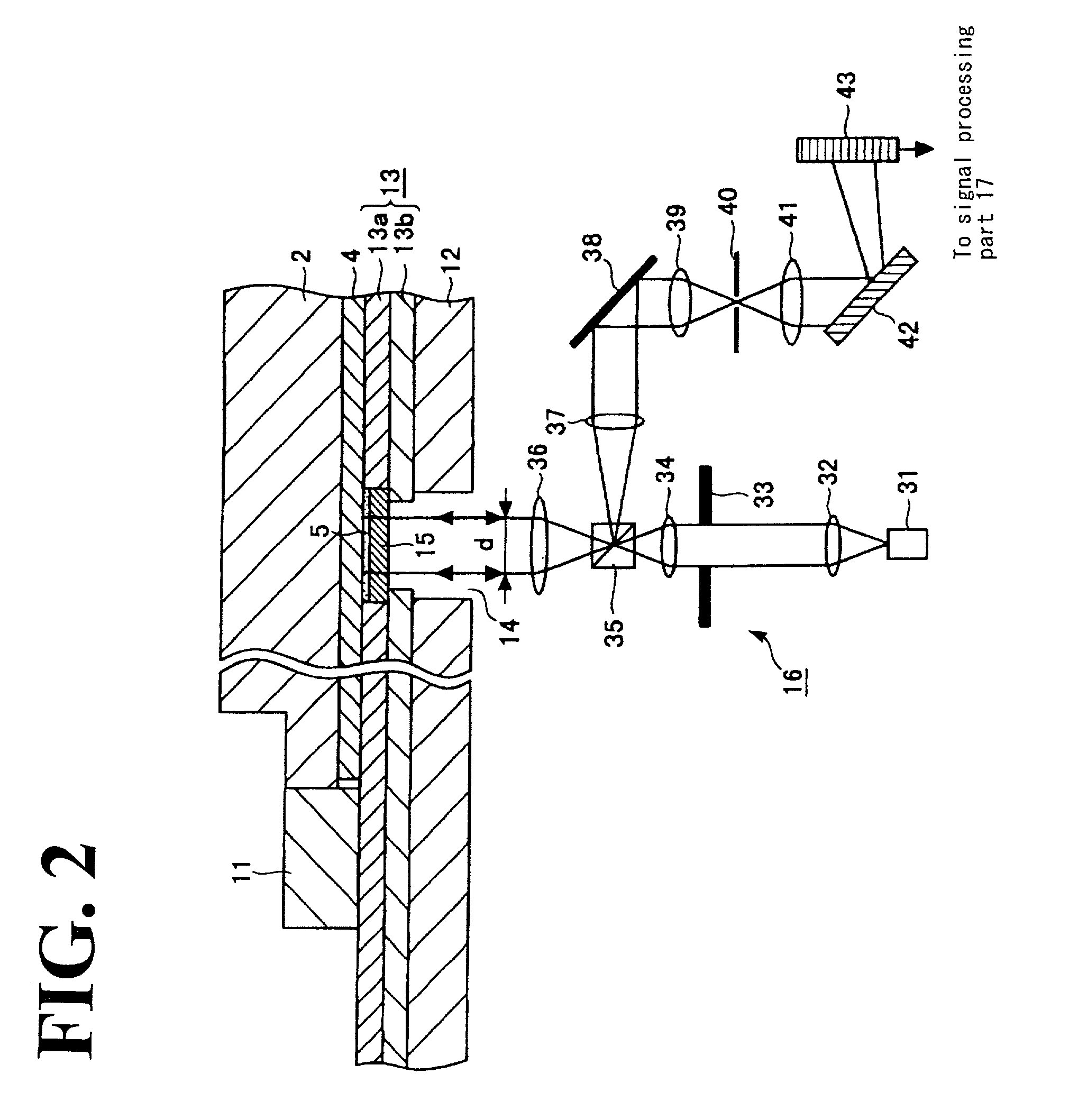
[0161] Experimental Example 2 relates to the above-mentioned third working configuration. In this experimental example, an IC1000 polishing pad and Suba400 polishing pad manufactured by Rodel Co., were used as the polishing pads 13a and 13b in the polishing apparatus shown in FIG. 4. The sizes of the two opening parts in the polishing pad 13a were respectively set at 60 mm.times.20 mm, and the sizes of the two opening parts in the polishing pad 13b were respectively set at 50 mm.times.10 mm. The surfaces of the transparent acrylic windows 15 and 115 were recessed 0.2 mm from the surface of the polishing pad 13a. The spacing of the centers of the windows 15 and 115 and the spacing of the centers of the opening parts 14 and 114 in the platen 12 were respectively set at 100 mm. A member in which aluminum was vacuum-evaporated to a thickness of 2 .mu.m as a metal film 52 on the surface of a transparent acrylic resin member 51 was used as the reflective body 50.
[0162] As in Experimental ...
PUM
| Property | Measurement | Unit |
|---|---|---|
| Pressure | aaaaa | aaaaa |
| Size | aaaaa | aaaaa |
| Ratio | aaaaa | aaaaa |
Abstract
Description
Claims
Application Information