Pre-divider architecture for low power in a digital delay locked loop
a delay lock and pre-divider technology, applied in the field of semiconductor memory, can solve the problems of limited maximum operational frequency of dll, significant power requirement, and reduced accuracy of read clock
- Summary
- Abstract
- Description
- Claims
- Application Information
AI Technical Summary
Problems solved by technology
Method used
Image
Examples
Embodiment Construction
[0029] This invention relates to semiconductor memories with delay lock loop including feedback for synchronizing a system clock with data output lines and reduces power usage. The invention conserves power using an input pre-divider circuit in a delay lock loop (DLL) circuit, preferably in SDRAM devices.
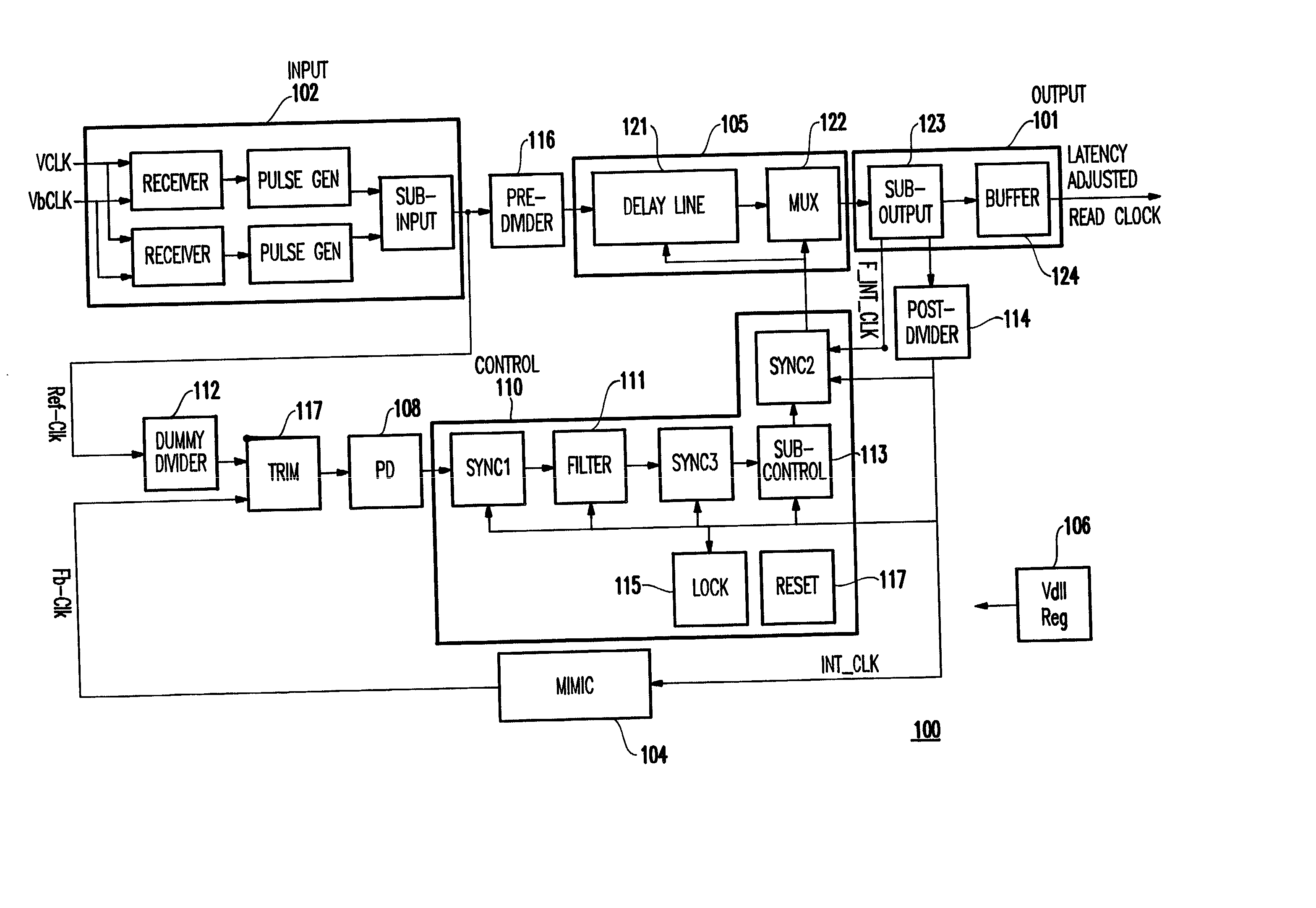
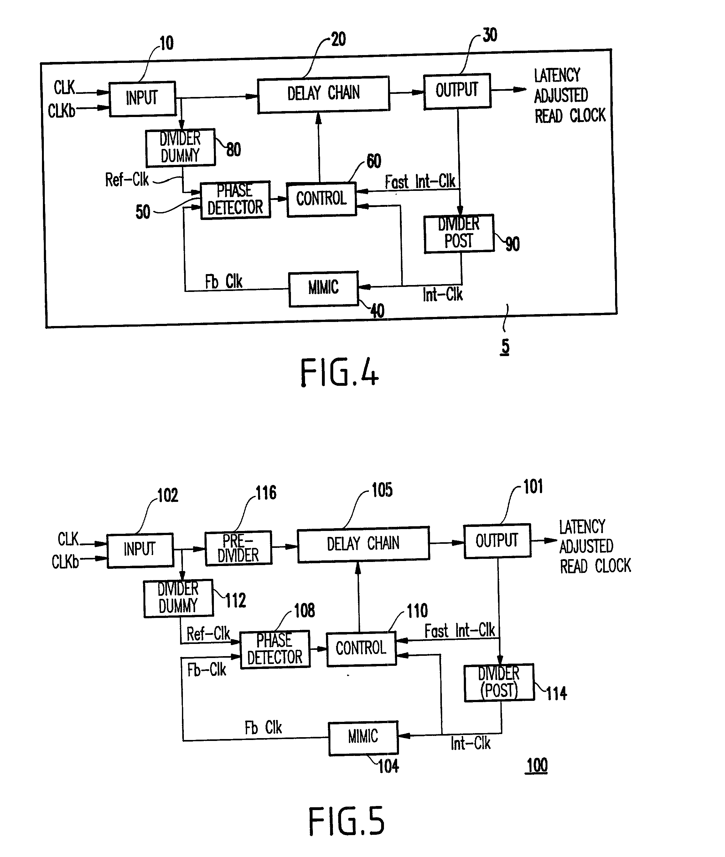
[0030] Referring now in specific detail to the drawings in which like reference numerals and block identification identify similar or identical elements throughout the several views, and initially to FIG. 5, an improved power conserving DLL circuit 100 is shown. The DLL circuit includes an input circuit 102, pre-divider 116, delay chain (line) 105 and output 101 which form the "primary signal" path leading from system input clock signals(CLK / CLKb) to DLL output signal (latency adjusted read clock signal). In addition to the Primary signal path the DLL contains two sub-paths which create a closed loop feedback system. These two sub-paths travel distinctly different routes inside the ...
PUM
 Abstract
Description
Claims
Application Information


