Structure and method for forming a multilayered structure

Inactive Publication Date: 2002-10-17
FUJITSU LTD
View PDF53 Cites 15 Cited by
  • Summary
  • Abstract
  • Description
  • Claims
  • Application Information

AI Technical Summary

Problems solved by technology

Unfortunately, staggering the via structures can consume valuable area in a multilayer circuit structure and can increase the signal run length.
This c

Method used


Image

  • Structure and method for forming a multilayered structure
  • Structure and method for forming a multilayered structure
  • Structure and method for forming a multilayered structure

Examples


Embodiment Construction

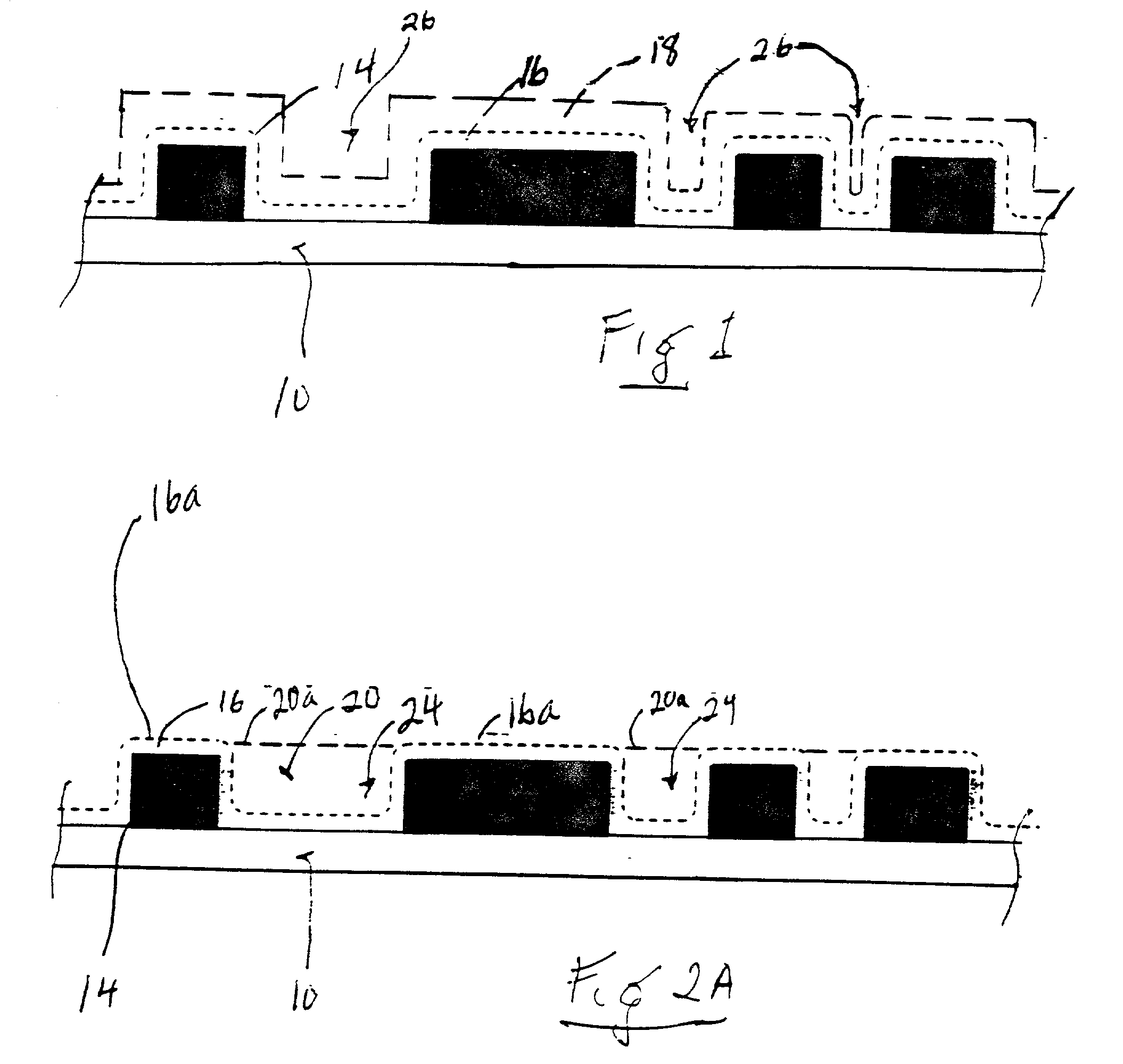
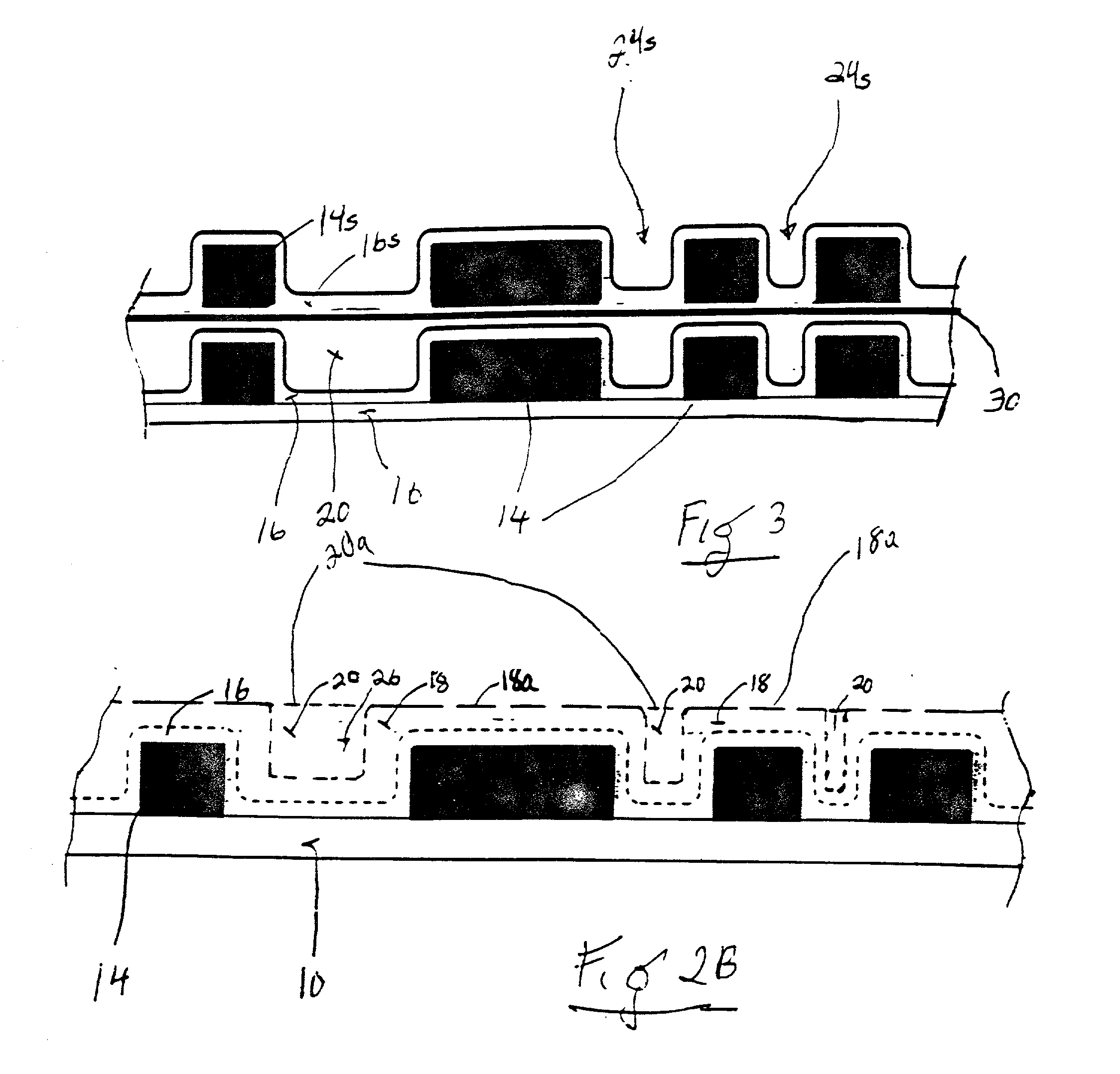
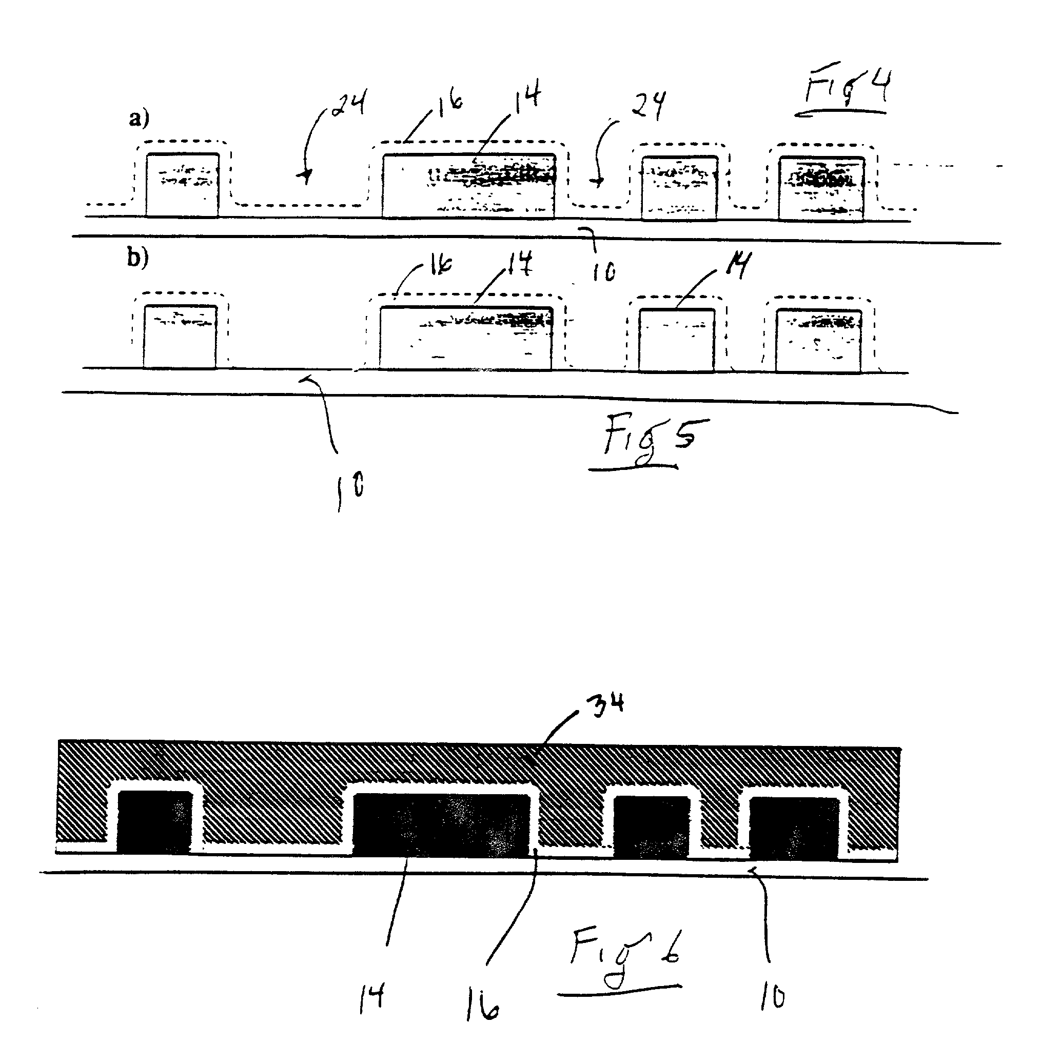
[0082] Referring in detail now to the drawings, there is seen in FIGS. 1-22 various embodiments of a structure and method for making a low dielectric constant MCM. Structures and methods of the type illustrated in FIGS. 1-22 are of priority of future generation MCM's as they will enable gigahertz speed products without huge losses, noise, and delays. The advantages of a low dielectric constant MCM of the various embodiments of the present invention are: (1) higher performance MCMs may be made with lower dielectric constants; (2) reduces amount of chemical mechanical polishing (CMP) required by using only conformal dielectric coatings in the MCMs; (3) enables better dielectric-layer adhesion than possible with only one type of dielectric polymer because of using two or more dielectric polymers; and (4) enables controlled impedance structures. A dielectric constant is a value serving as an index of the ability of the dielectric material(s) (e.g., polymers) to resist the transmission o...


PUM

PropertyMeasurementUnit
Temperatureaaaaaaaaaa

Abstract

Improved methods for forming multilayer circuit structures are disclosed. In some embodiments, conductive layers, dielectric layers and conductive posts can be formed on both sides of a circuitized core structure. The conductive posts are disposed in the dielectric layers and can be stacked to form a generally vertical conduction pathway which passes at least partially through a multilayer circuit structure. The formed multilayer circuit structures can occupy less space than corresponding multilayer circuit structures with stacked via structures.

Description

[0001] This is a continuation-in-part patent application of patent applications having Ser. No. 09 / 429,854, filed Oct. 28, 1999, and Ser. No. 09 / 956,605, filed Sep. 18, 2001. Benefit of the earlier filing dates is claimed for all common subject matter.[0002] 1. Field of the Invention[0003] The present invention is related to multilayered circuit structure. More specifically, the present invention provides a structure and method for producing or forming a multilayered circuit structure.[0004] 2. Description of the Prior Art[0005] Multilayer circuit structures can be used to electrically communicate two or more electrical devices such as two or more computer chips. Multilayer circuit structures typically contain multiple conductive layers separated by one or more dielectric layers. Via structures disposed in apertures in the dielectric layers provide conductive paths so that electrical signals can pass from one conductive layer to another conductive layer. Multiple via structures in s...

Claims


Application Information

Patent Timeline
IPC IPC(8): H01L21/48H05K3/00H05K3/10H05K3/24H05K3/46
CPCH01L21/486Y10T428/24066H01L2221/68345H01L2224/16237H01L2924/01013H01L2924/01027H01L2924/01029H01L2924/0103H01L2924/01042H01L2924/01046H01L2924/01047H01L2924/01051H01L2924/0106H01L2924/01074H01L2924/01075H01L2924/01078H01L2924/01079H01L2924/01082H01L2924/01322H01L2924/01327H01L2924/14H01L2924/15311H01L2924/19041H01L2924/30105H01L2924/30107H01L2924/3011H05K3/0035H05K3/108H05K3/243H05K3/4602H05K3/4647H05K2203/066H05K2203/0733H05K2203/1383H01L2224/81193H01L2224/81141H01L2924/00013H01L2924/01005H01L2924/01006H01L2924/01023H01L2924/01033H01L2924/01087H01L24/96Y10T428/24174H01L2224/13099H01L2924/12042H01L2224/05573H01L2224/05568H01L2924/00H01L2224/05644H01L2924/00014H01L2224/05647
Inventor ZHANG, LEIJIANG, HUNT HANG
Owner FUJITSU LTD
Why Eureka
Try Eureka