Semiconductor laser device and method for fabricating the same

a laser device and semiconductor technology, applied in semiconductor lasers, lasers, laser details, etc., can solve the problems of reducing the laser emission efficiency, increasing the leakage current path width, and worsening the output characteristic and linearity of the current-voltage characteristi

Inactive Publication Date: 2002-10-31
FURUKAWA ELECTRIC CO LTD
View PDF0 Cites 15 Cited by
  • Summary
  • Abstract
  • Description
  • Claims
  • Application Information

AI Technical Summary

Problems solved by technology

Similarly, in the fabrication of the buried semiconductor laser device formed on the p-type substrate, an n-type InP contact layer is excessively grown to be in contact with an n-type InP contact layer, and a leakage current path width is increased.
As a result, the increased leakage current lowers the laser emission efficiency to worsen the output characteristic and the linearity of the current-voltage characteristic, and the buried semiconductor laser device with the higher output can be hardly fabricated with the excellent reproducibility.

Method used


Image

  • Semiconductor laser device and method for fabricating the same
  • Semiconductor laser device and method for fabricating the same
  • Semiconductor laser device and method for fabricating the same

Examples


embodiment 2

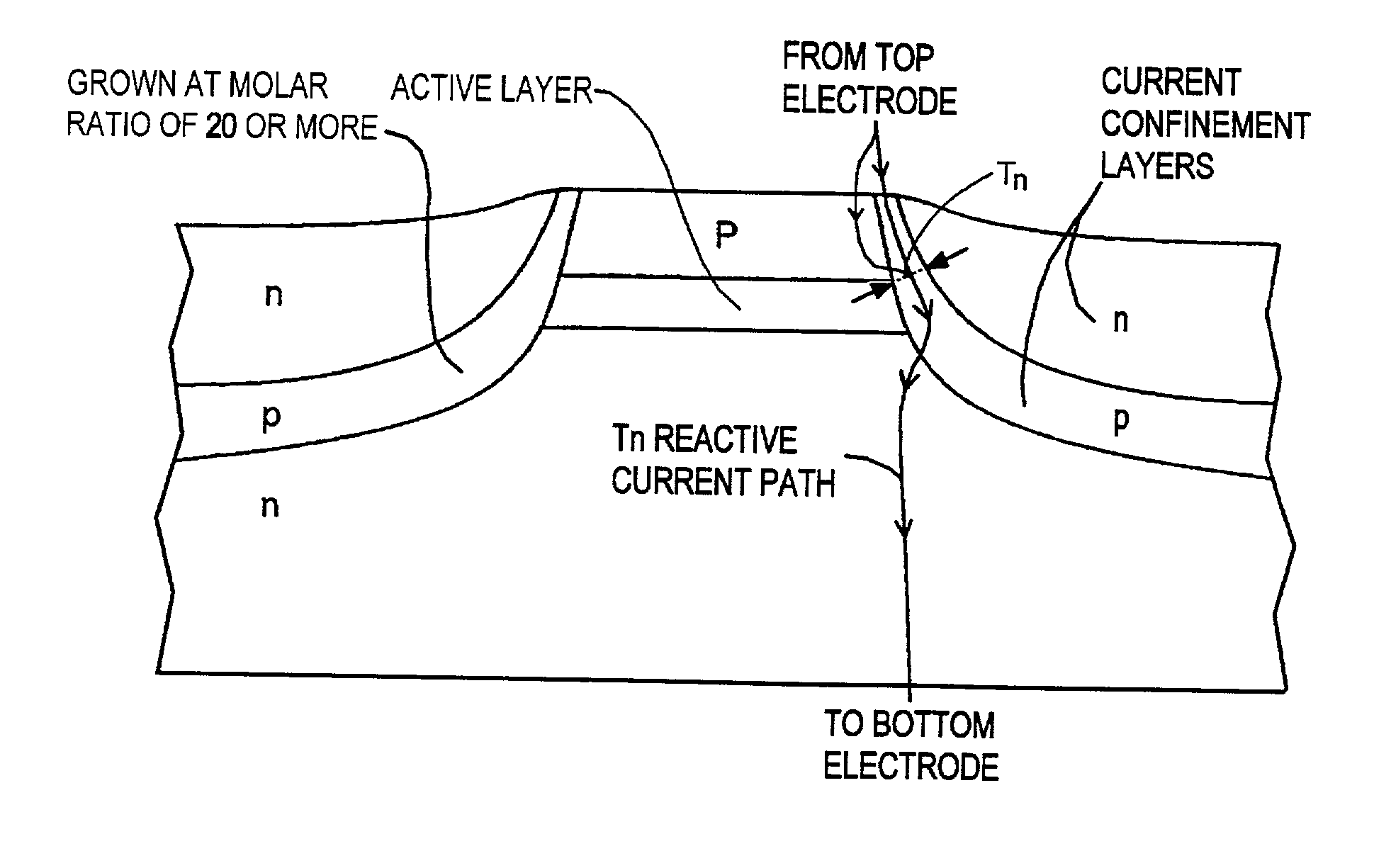
[0036] FIG. 3B shows a buried semiconductor device which is built upon a p-type substrate and which has a three-layer current-confinement structure disposed on either side of a light-guiding mesa ridge (Embodiment 2). The mesa ridge has a p-type bottom cladding layer formed over the p-type substrate, an active layer formed over the bottom cladding layer, and an n-type top cladding layer formed over the active layer. The active layer generally comprises two or more sub-layers. The current confinement structure comprises a p-type separation layer formed over the p-type substrate and p-type bottom cladding layer, an n-type current blocking layer formed over the p-type separation layer, and a p-type current blocking layer formed over the n-type current blocking layer. When a voltage is applied between the top and bottom electrodes of the laser to place the device in an operating (lasing) state, a leakage current path is formed between the top and bottom electrodes which allows current t...

example 1

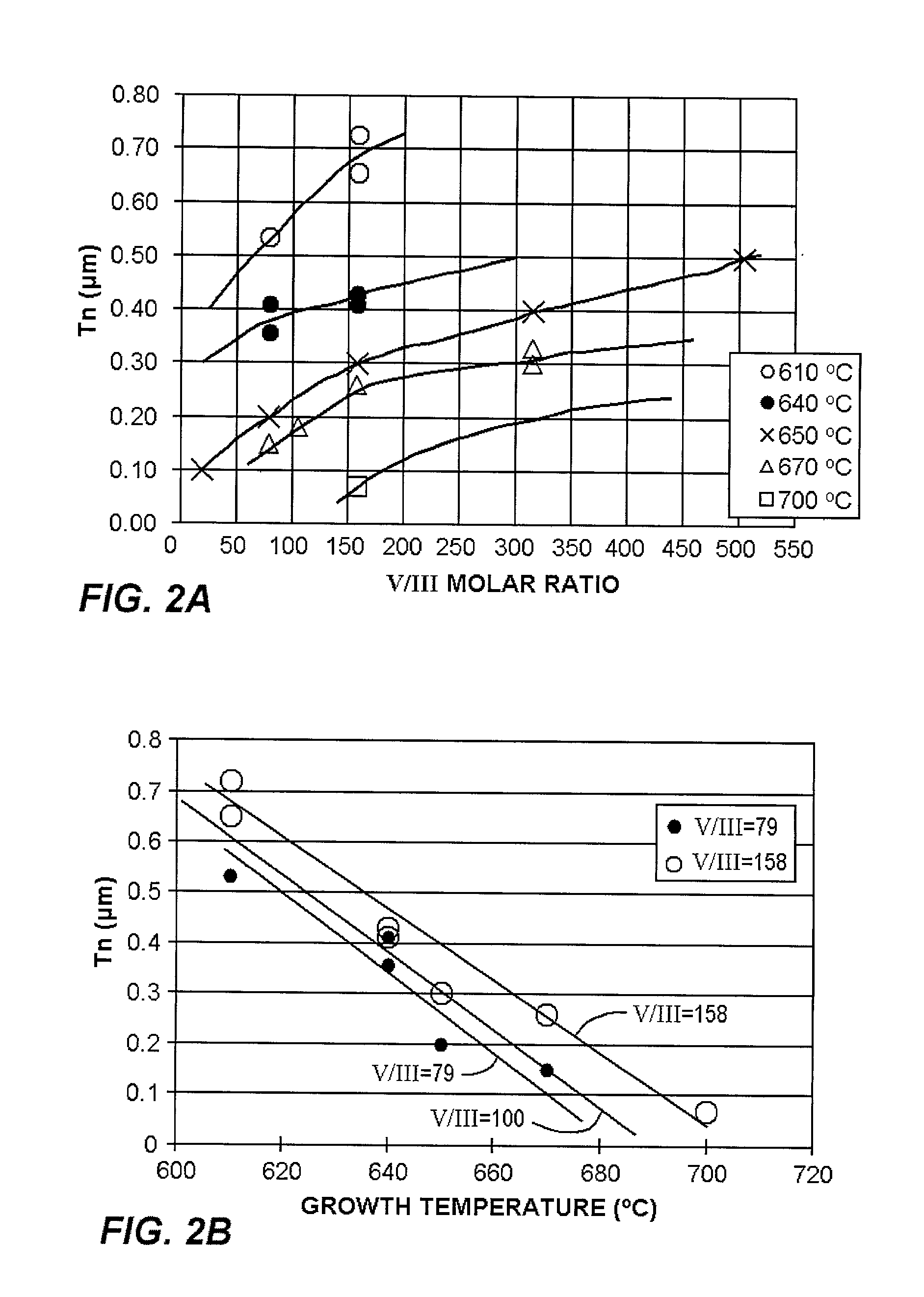
[0087] Example 1 uses the above fabrication steps with the p-type InP current blocking layer 59 and the n-type InP current blocking layer 60 being formed at the growth temperature of 650.degree. C. and at the molar ratios of 80 and 158, respectively, for filling the space around the mesa structure 58. After the top cladding layer 61 and the cap layer 62 were sequentially formed, the two electrodes 63, 64 were formed thereon and on the bottom surface of the substrate 51. Then, the obtained structure was cleaved, a low reflection film and a high reflection film were formed on respective ones of the cleaved surfaces, thereby fabricating a semiconductor laser device of Example 1 having an emission wavelength range from 1.28 .mu.m to 1.63 .mu.m.

[0088] As shown in Table 2, the leakage current path width "Tn" observed with an electron microscope was 0.19 .mu.m.

2 TABLE 2 Leakage Molar Ratio Molar Ratio Current of p-type of n-type Path Conduct-Current Current Width ivity of Growth Blocking B...

examples 2 and 3

[0089] Buried semiconductor laser devices of Examples 2 and 3 having the emission wavelength range from 1.28 .mu.m to 1.63 .mu.m were fabricated by using the same conditions as those of Example 1 except that the molar ratios of the raw material gas for forming the p-type InP current blocking layer 59 and the n-type InP current blocking layer 60 were shown in Table 2, which were different from those of Example 1. The leakage current path widths "Tn" thereof were 0.21 .mu.m and 0.41 .mu.m, respectively, as shown in Table 2.


PUM


Abstract

A method for fabricating a buried semiconductor laser device including the steps of: forming a mesa structure including a bottom cladding layer, an active layer and a top cladding layer overlying an n-type semiconductor substrate; and forming a current confinement structure by growing a p-type current blocking layer and an n-type current blocking layer on each side surface of the mesa structure and on a skirt portion extending from the each side surface, the p-type current blocking layer being fabricated by using a raw material gas containing a group III element gas and a group V element gas at a molar ratio between 60 and 350 inclusive. In this method, the semiconductor laser device including the current confinement structure with the specified leakage current path width can be fabricated with the excellent reproducibility.

Description

[0001] The present application claims benefit of priority under 35 U.S.C. .sctn.119 to the following Japanese patent Applications Nos. 2000-364387 (filed on Nov. 30, 2000) and 2001-360940 (filed on Nov. 27, 2001), each of which are incorporated herein by reference.[0002] (a) Field of the Invention[0003] The present invention relates to a semiconductor laser device and a method for fabricating the same, and more particularly to a so-called buried semiconductor laser device having a higher laser emission efficiency and a higher reproducibility of a current-optical output characteristic.[0004] (b) Description of the Related Art[0005] A semiconductor laser device having a lower threshold current density and a higher laser emission efficiency is desirable. A strained quantum well semiconductor laser device having a hetero-structure and a pair of current blocking layers is attracting public attention because of the excellent characteristics thereof. The semiconductor laser having a pair o...

Claims


Application Information

Patent Timeline
Patent Type & Authority Applications(United States)
IPC IPC(8): H01S5/22H01S5/227H01S5/323
CPCH01L21/02392H01S2304/04H01L21/02505H01L21/02543H01L21/02546H01L21/02576H01L21/02579H01L21/0262H01L21/02664H01S5/2206H01S5/2222H01S5/2223H01S5/227H01S5/2275H01S5/32308H01L21/02461
Inventor HONKAWA, YUKIOONO, TAKAHIROHATTORI, SATOSHISATO, YOSHIHIRO
Owner FURUKAWA ELECTRIC CO LTD
Why Eureka
Try Eureka