Method for manufacturing a pair of complementary masks

a technology of complementary masks and masks, applied in the field of complementary mask manufacturing, can solve the problems of reducing affecting the processing accuracy of masks, and unable to form a particular pattern opening in silicon substrates,

Inactive Publication Date: 2002-11-14
RENESAS ELECTRONICS CORP
View PDF14 Cites 3 Cited by
  • Summary
  • Abstract
  • Description
  • Claims
  • Application Information

AI Technical Summary

Problems solved by technology

The EB technique including the new-developed cell projection type patterning, however, has yet an insufficient throughput due to the consecutive depiction of the patterns, irrespective whether these patterns are formed by a single pattern basis or a single area basis.
In general, in the case of the EPL mask implemented by a stencil mask, it is difficult to form a particular pattern opening in the silicon substrate if the particular pattern opening involves a lower mechanical strength of the mask.
The difference in the pattern density between the complementary masks A and B also degrades the accuracy of the mask processing, especially in the...

Method used


Image

  • Method for manufacturing a pair of complementary masks
  • Method for manufacturing a pair of complementary masks
  • Method for manufacturing a pair of complementary masks

Examples


Embodiment Construction

[0032] Now, the present invention is more specifically described with reference to accompanying drawings.

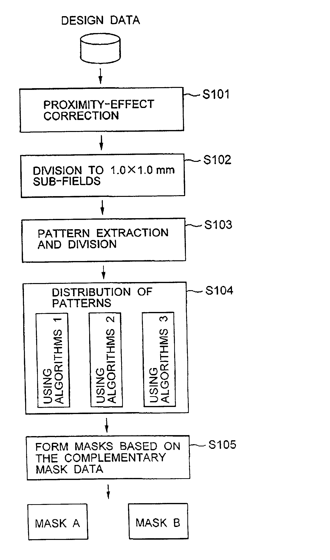
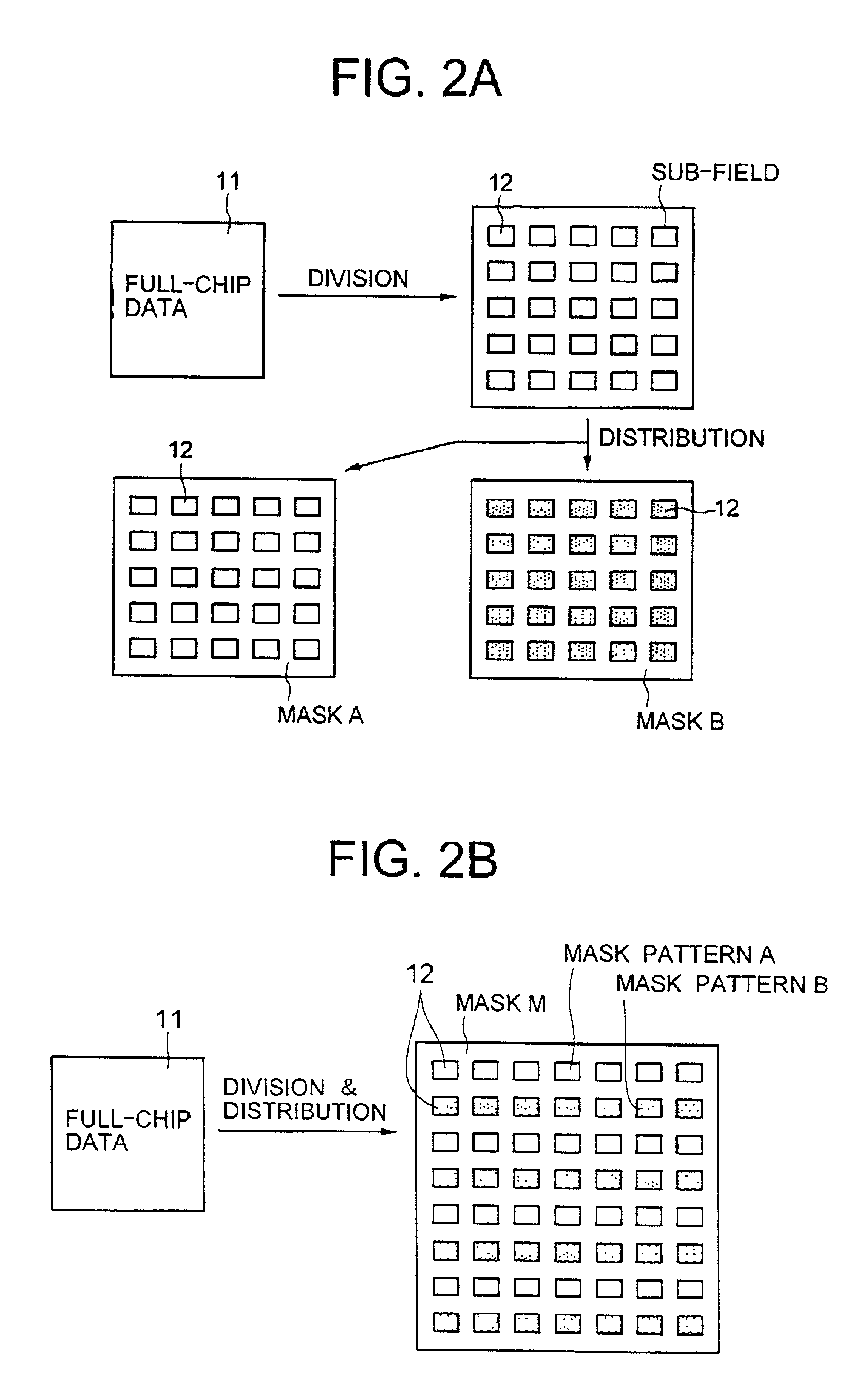
[0033] Referring to FIG. 5, a process for manufacturing a pair of complementary EPL masks according to an embodiment of the present invention includes a first (proximity effect correction) step S101, wherein the full-chip data of a semiconductor device obtained from the design data is subjected to a proximity effect correction to resize or reshape the patterns, a second (sub-field division) step S102, wherein the corrected data is divided into a plurality of sub-field data each having, for example, a 1.0 mm.times.1.0 mm square size, a third (pattern division) step S103, wherein each sub-field data is subjected to pattern extraction for extracting a particular pattern data, such as donut pattern data, and dividing the extracted pattern data into a plurality of rectangular pattern data, a fourth (pattern distribution) step S104, wherein the pattern data are distributed to a pair of...


PUM


Abstract

A method for manufacturing a pair of complementary masks for use in an electron projection lithographic (EPL) technique uses an algorithm for distributing the design data to a pair of EPL masks. The algorithm allocates a positive sign or negative sign to each of the pattern data, summation of the areas of the pattern data having positive signs while subtracting the areas of the pattern data having negative signs, for obtaining a minimum of the sum. One or more of initial combination of the signs is prepared and the vicinity of the initial combination is calculated therefrom for obtaining an optimum combination.

Description

[0001] (a) Field of the Invention[0002] The present invention relates to a method for manufacturing a pair of complementary masks and, more particularly, to an improvement of the method for manufacturing a pair of complementary masks for use in an electron beam (EB) lithography.[0003] (b) Description of the Related Art[0004] Along with the development in higher integration of semiconductor devices, lithographic techniques are ever directed to finer design-rule patterning. In this situation, X-ray and EB lithographic techniques attract larger attentions instead of the conventional lithographic technique using ultraviolet-ray having a longer wavelength.[0005] In the EB lithography, an objective device pattern is formed by iterative operation of deflecting an electron beam to form a pattern on a specified area, and then moving the wafer stage to effect forming a pattern on a different area of the wafer. The deflection of the electron beam is conducted based on the writing data obtained...

Claims


Application Information

Patent Timeline
IPC IPC(8): G03F1/20G03F1/68H01L21/027
CPCG03F1/20H01L21/027
Inventor YAMADA, YASUHISATAKADA, KENICHI
Owner RENESAS ELECTRONICS CORP
Why Eureka
Try Eureka